Executive Summary
- IBM achieved the industry’s first 1-megabit DRAM production 40 years ago, marking a 16x density increase.
- The breakthrough transitioned the computing industry from the 64-kilobit era to high-density memory architectures.
- This legacy shift established the foundation for modern memory scaling laws and current HBM architectures.
Strategic Deep-Dive
The 1-Megabit Inflection Point
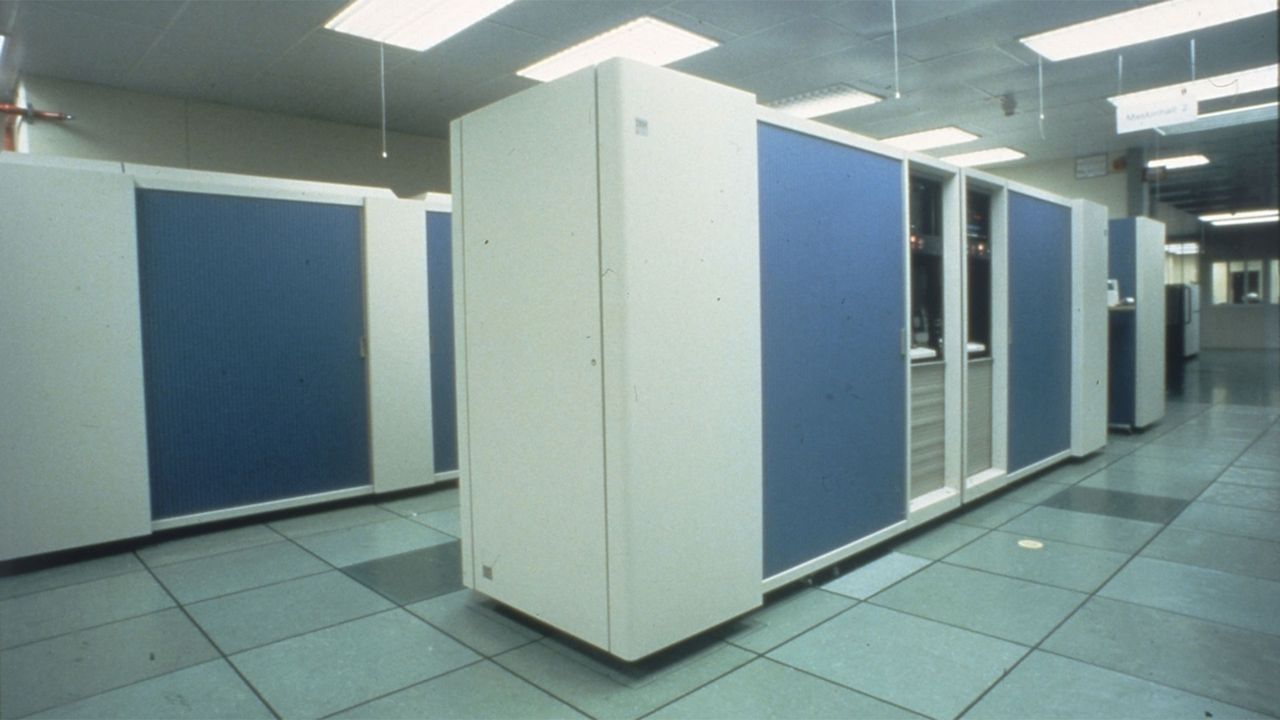
Forty years ago, IBM achieved a critical milestone in semiconductor history by successfully moving from 64-kilobit (Kb) DRAM chips to the 1-megabit (Mb) density threshold. At the time, this represented a quantum leap in memory capacity, effectively quadrupling the density of the then-standard 256Kb chips and providing a 16x improvement over the older 64Kb generation.
Technical Specifications and Scaling
The transition to 1Mb DRAM was not merely a capacity increase; it required fundamental shifts in lithography and manufacturing processes. By shrinking circuit features to the sub-micron level, IBM addressed the ‘memory wall’ that threatened to stagnate the performance of early mainframe systems. This era introduced the necessity for cleaner fabrication environments and more precise ion implantation techniques, setting the stage for the next four decades of Moore’s Law application in memory.
Business Risks and Market Dynamics
In 1984, the transition carried significant risk. High-density DRAM production suffered from low yields, making early 1Mb chips prohibitively expensive. Manufacturers faced the ‘yield-to-cost’ trap: the capital expenditure required to retool facilities for 1Mb production risked insolvency if yields did not stabilize quickly.
IBM’s ability to internalize this production shielded it from supply chain volatility, a strategy that remains a blueprint for modern hyperscalers developing proprietary silicon.
Future Outlook: From Megabits to High Bandwidth
The 1Mb breakthrough was the precursor to the current era of High Bandwidth Memory (HBM). While the industry has moved from megabits to gigabits and terabytes, the architectural challenges remain identical: balancing thermal management, power leakage, and data density. As we reach the physical limits of traditional DRAM, the industry is once again looking toward stacked memory architectures that echo the density-driven ambitions of the 1984 IBM engineering team.
Strategic Insights
IBM’s 1984 move serves as a historical reminder that memory density is the primary bottleneck for compute performance. Just as the 1Mb chip enabled the personal computing revolution, today’s race for HBM3e and beyond is the singular constraint on generative AI scaling. Hardware dominance is, and has always been, a function of memory throughput.