Executive Summary
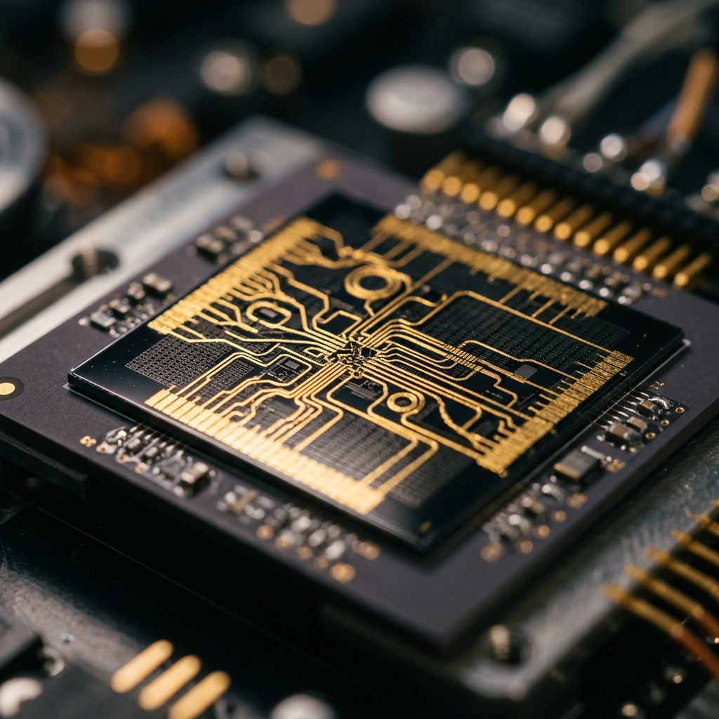
- India has officially entered the high-end semiconductor race with the groundbreaking of its first 3D packaging unit in Odisha. Focusing on heterogeneous integration, this facility positions India as a strategic hub for AI, defense, and aerospace hardware.
Strategic Deep-Dive
On April 19, 2026, India marked a historic milestone with the groundbreaking of its first advanced 3D chip packaging unit in Odisha. This move signals India’s strategic pivot into the high-end semiconductor supply chain, specifically focusing on heterogeneous integration—a critical technology for bypassing the limitations of Moore’s Law through chiplet-based architectures. By prioritizing advanced packaging over the prohibitively expensive leading-edge lithography, India is positioning itself as a specialized hub for AI, aerospace, and defense hardware.
This facility is expected to disrupt the long-standing East Asian monopoly in the OSAT sector, offering global tech firms a viable alternative for high-performance computing needs. From an analyst’s perspective, this is a calculated leap toward technological sovereignty, providing the foundational infrastructure to support India’s long-term ambitions as a global semiconductor powerhouse.


