Executive Summary
- Spanish startup Wooptix is challenging the metrology market with its ‘Phemet’ optical inspection system. Targeting 2028 for full foundry integration, the firm aims to enhance yield in advanced nodes through innovative European-made toolsets.
Strategic Deep-Dive
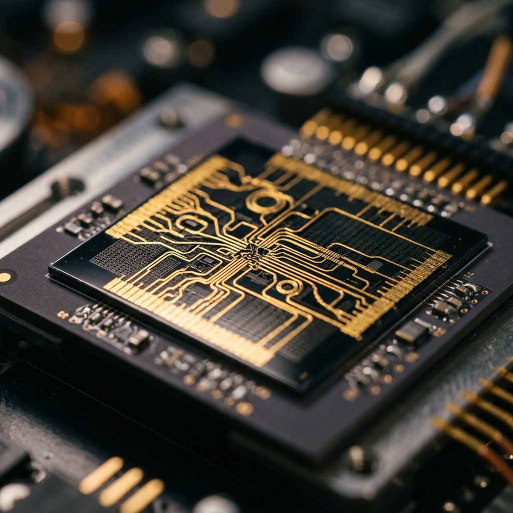
Wooptix, a burgeoning Spanish startup in semiconductor metrology, has unveiled its ‘Phemet’ system, marking a significant entry into the high-precision inspection market. Developed in collaboration with leading European research centers and wafer manufacturers, Phemet utilizes advanced optical techniques to map wafer surface topography with sub-nanometer accuracy. As the industry pushes toward 2nm and beyond, the ability to identify atomic-level defects rapidly is critical for maintaining yield.
Wooptix’s roadmap targets integration into major global foundries by 2028, positioning itself as a vital European alternative to established metrology vendors. This development aligns with the EU Chips Act’s goal of fostering a resilient, “homegrown” semiconductor tool chain. By expanding Europe’s expertise from lithography into optical inspection, Wooptix is strengthening the continent’s strategic autonomy in the global chip ecosystem.


