Executive Summary
- The second quarter of 2026 has become a defining moment for Samsung Electronics’ memory division, marked by a sharp divergence in its product roadmap. While the company is successfully capturing the lucrative automotive silicon market through a ramp-up in GDDR6 supply for Tesla, it is simultaneously retreating from its cutting-edge 1d DRAM mass production plans. This “retreat-and-refocus” strategy highlights the immense technical barriers of the sub-10nm DRAM era and suggests a shift from volume-driven leadership to quality-driven profitability.
Strategic Deep-Dive
Introduction: Samsung’s High-Stakes Strategic Pivot
The second quarter of 2026 has become a defining moment for Samsung Electronics’ memory division, marked by a sharp divergence in its product roadmap. While the company is successfully capturing the lucrative automotive silicon market through a ramp-up in GDDR6 supply for Tesla, it is simultaneously retreating from its cutting-edge 1d DRAM mass production plans. This “retreat-and-refocus” strategy highlights the immense technical barriers of the sub-10nm DRAM era and suggests a shift from volume-driven leadership to quality-driven profitability.
Technical Deep-Dive: Automotive Resilience vs. 1d Yield Failure
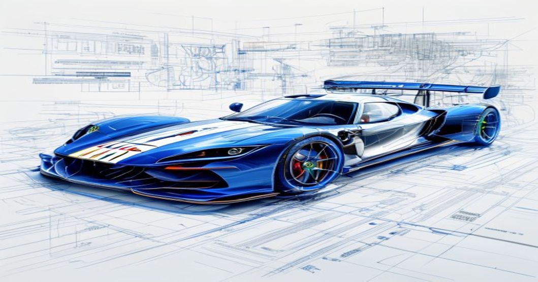
Samsung’s expansion of GDDR6 production for Tesla, starting in April 2026, is a significant technical validation. Automotive environments are brutal; chips must withstand extreme temperature fluctuations and vibration for a 15-year lifecycle. Samsung’s GDDR6, optimized for high bandwidth and low power, has become the backbone of Tesla’s next-generation FSD (Full Self-Driving) computers.
These chips are essential for processing the massive data streams from 360-degree camera arrays in real-time. By prioritizing this high-margin sector, Samsung is building a resilient revenue stream that is less susceptible to the cyclical volatility of the PC and smartphone markets.
Contrast this with the failure of the 1d DRAM mass production plan. The 1d node (the fourth generation of 10nm-class DRAM) represents the bleeding edge of memory scaling. Reports indicate that Samsung has hit a “yield wall,” where the number of functional chips per wafer is insufficient for commercial viability.
Technically, the 1d transition requires extreme precision in capacitor formation—making them tall and thin enough to hold a charge without collapsing or leaking current into adjacent cells. The move toward high-k dielectrics and possibly EUV for more layers in the 1d process has introduced manufacturing complexities that have not yet been stabilized. Halting production now prevents a “sunk cost” fallacy where Samsung would lose money on every wafer produced.
Market Impact: A Shift in the Memory Hierarchy
This tactical halt provides a temporary window for SK Hynix and Micron to claim a lead in the next-generation DRAM market. However, Samsung’s focus on GDDR6 and HBM (High Bandwidth Memory) indicates that the company is reallocating its R&D and CAPEX toward “specialized memory” rather than “commodity memory.” In the AI and automotive era, the profitability of a specialized 16Gb GDDR6 chip far exceeds that of a standard DDR5 module. This move may actually improve Samsung’s 2026 balance sheet by cutting losses in the low-yield 1d segment and maximizing output in proven, high-demand segments.
Future Outlook: Re-engineering for the 1e Era
Samsung’s “halting” of 1d DRAM is likely a tactical reset rather than a permanent abandonment. We expect the company to spend the next 12-18 months re-engineering its process flow, potentially skipping some iterations of 1d to move directly toward “1e” or integrating more advanced 3D DRAM architectures. During this recalibration period, the Tesla partnership will serve as a critical stabilizer, proving that Samsung remains the gold standard for high-reliability, high-performance specialized memory.