Executive Summary
- The “Strix Halo” architecture marks the first time AMD has brought its successful chiplet strategy to the high-end mobile APU market. By disaggregating the CPU, GPU, and I/O components into separate dies within a single package, AMD has bypassed the scaling limits of traditional monolithic designs. This overview explores the structural shift to a multi-die approach and the technical hurdles of interconnect power and latency in mobile form factors.
Strategic Deep-Dive
The transition from monolithic to chiplet-based architectures is the most significant structural change in the history of AMD’s mobile processors. Traditional mobile APUs, such as the Phoenix or Strix Point series, rely on a single die where every component—CPU cores, GPU clusters, and memory controllers—is etched onto one piece of silicon. While monolithic designs offer excellent latency and lower idle power, they are incredibly difficult to scale.
As the demand for larger GPUs grows, the size of a monolithic die would become so large that manufacturing yields would plummet, and costs would skyrocket. Strix Halo solves this by using a “disaggregated” approach: separate Core Complex Dies (CCDs) for the Zen 5 CPU and a massive Graphics Compute Die (GCD) for the RDNA 3.5 GPU.
A critical challenge in this chiplet transition is the “Interconnect Power Cost.” In a monolithic chip, data travels through short, efficient metal traces. In a chiplet design, data must travel across the Infinity Fabric interconnect between separate physical dies. This typically consumes significantly more energy per bit.
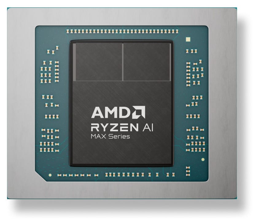
AMD has addressed this for the Strix Halo mobile envelope by evolving the Infinity Fabric On-Package (IFOP) technology. By using higher-density packaging and optimizing the voltage rails for the interconnect, AMD has managed to bring the power penalty down to a level manageable for high-end laptops. This allows the Ryzen AI MAX series to maintain a high level of performance-per-watt while housing up to 16 cores—a feat previously reserved for desktop CPUs or high-heat mobile workstations.
Furthermore, the chiplet strategy allows AMD to use “mixed-node” manufacturing. The Zen 5 CCDs can be manufactured on a performance-optimized 3nm or 4nm node to maximize clock speeds, while the I/O and cache sections of the GCD can use a more cost-effective node. This flexibility is what makes Strix Halo a “Halo” product—it enables a level of compute and graphics density that is physically impossible on a single-die mobile processor.
The implications for industrial design are profound. Laptop manufacturers can now create 14-inch or 16-inch devices with “console-level” power without the need for the complex, dual-cooler setups required for separate CPU and discrete GPU chips. This marks the beginning of an era where the distinction between “integrated” and “discrete” performance is no longer defined by the physical packaging, but by the architectural ambition of the SoC.