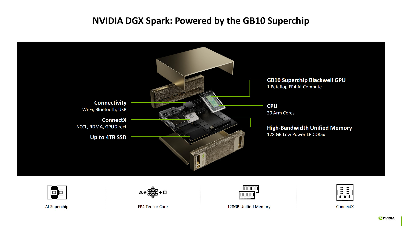
Executive Summary
- Nvidia’s introduction of the GB10 architecture represents a seismic shift in how the industry views integrated graphics. No longer are iGPUs relegated to being “display adapters” for office spreadsheets; the GB10 aims to fulfill the “Big iGPU” vision—bringing the massive compute density of Nvidia’s discrete GPU (dGPU) lineup directly into the processor package. Leveraging IP blocks from the Blackwell and Hopper architectures, Nvidia is attempting to create a silicon monster that can rival mid-range discrete cards in gaming and AI workloads while maintaining the footprint of a standard SoC.
Strategic Deep-Dive
Nvidia’s introduction of the GB10 architecture represents a seismic shift in how the industry views integrated graphics. No longer are iGPUs relegated to being “display adapters” for office spreadsheets; the GB10 aims to fulfill the “Big iGPU” vision—bringing the massive compute density of Nvidia’s discrete GPU (dGPU) lineup directly into the processor package. Leveraging IP blocks from the Blackwell and Hopper architectures, Nvidia is attempting to create a silicon monster that can rival mid-range discrete cards in gaming and AI workloads while maintaining the footprint of a standard SoC.
The primary hurdle for any large-scale iGPU is the memory bandwidth wall. In a traditional dGPU setup, the processor is paired with dedicated GDDR6X or HBM memory, providing hundreds of gigabytes per second of dedicated throughput over a 128-bit or 256-bit bus. The GB10, however, must share its memory with the CPU, usually limited by the constraints of LPDDR5x or DDR5 system memory.
Even with high-speed LPDDR5x-8533, the available bandwidth for a massive GPU core is significantly lower than that of its discrete counterparts. To combat this, Nvidia has implemented a massive L2 cache—likely exceeding 32MB—which acts as a high-speed buffer to minimize the number of times the GPU has to reach out to the relatively slow system RAM.
Beyond raw cache size, the GB10 utilizes advanced Delta Color Compression (DCC) and other lossless compression techniques to squeeze more effective bandwidth out of the system memory. By compressing data before it leaves the chip, Nvidia can effectively “amplify” the existing bandwidth, allowing the large number of CUDA cores in the GB10 to remain fed. This Unified Memory Architecture (UMA) also offers a massive advantage in latency: because the CPU and GPU share the same memory space, there is no need to copy large datasets over the high-latency PCIe bus.
This is a game-changer for AI inferencing and professional video editing, where large models or frames can be accessed instantly by both compute engines.
However, the “Big iGPU” strategy brings intense thermal challenges. Packing a high-performance GPU and a multi-core CPU onto the same die creates a thermal density nightmare. Nvidia must utilize aggressive power gating and granular frequency scaling to ensure the chip doesn’t exceed the Total System Power (TSP) limits of premium ultraportable laptops.
If successful, the GB10 will not only eliminate the need for entry-level dGPUs but will also redefine the performance-per-watt curves for the entire mobile PC industry, enabling “Pro” performance in form factors previously reserved for low-power ultrabooks.


