Executive Summary
- Technical deep-dive into the Blackwell B200 architecture featuring a 208-billion transistor dual-die design.
- Evaluation of the 1200W+ TDP and 192GB HBM3e integration for trillion-parameter model training.
- Strategic analysis of how Nvidia’s hardware-software synergy through CUDA remains an insurmountable barrier for competitors.
Strategic Deep-Dive
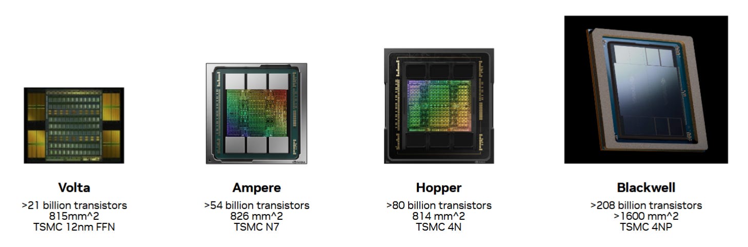
The transition from Nvidia’s Hopper architecture to the Blackwell B200 represents a monumental shift in semiconductor design, moving beyond incremental improvements to a unified platform strategy. The B200 is not merely a single processor but a sophisticated multi-die assembly featuring 208 billion transistors. By utilizing a high-speed, 10TB/s interconnect between two TSMC 4NP-processed dies, Nvidia has effectively bypassed the physical limits of single-reticle lithography.
This allows the B200 to function as a singular, massive GPU with 192GB of HBM3e memory, delivering a staggering 8TB/s of memory bandwidth. For senior architects, the most compelling advancement is the second-generation Transformer Engine, which introduces FP4 precision. This enables the B200 to achieve up to 20 Petaflops of compute, a nearly 5x increase over the H100’s FP8 performance, specifically tailored for the inference and training of trillion-parameter Large Language Models (LLMs).
However, the hardware’s raw power is only half of the story. Nvidia’s true strategic asset is the CUDA software moat, which has been meticulously expanded over two decades. The B200 reinforces this moat by ensuring seamless backward compatibility while introducing hardware-level optimizations for new software primitives.
As noted by Verda (formerly DataCrunch), the deployment of Blackwell clusters requires sophisticated infrastructure capable of handling a Thermal Design Power (TDP) exceeding 1200W per GPU. Verda’s transition to managing these high-density Blackwell units highlights the operational complexity that competitors struggle to match. While startups like Groq or Etched attempt to challenge Nvidia with specialized ASICs, they lack the software maturity that allows researchers to deploy new model architectures on B200 via CUDA with zero code refactoring.
The Blackwell platform further extends Nvidia’s reach into the networking domain with the integration of BlueField-3 DPUs and the Quantum-X800 InfiniBand platform. By controlling the entire stack—from the individual transistor to the rack-level NVLink Switch System—Nvidia has transformed from a chip vendor into a systems provider. This systemic approach significantly increases the Total Cost of Ownership (TCO) for customers attempting to switch to alternative silicon.
If a cloud provider migrates away from Nvidia, they do not just replace a GPU; they lose access to a decade of optimized libraries, debuggers, and a massive talent pool of CUDA-fluent engineers. The B200 is the ultimate manifestation of this “locked-in” ecosystem, providing a performance ceiling so high that the risk of migrating to unproven architectures becomes economically unjustifiable for most Tier-1 hyperscalers. Ultimately, the Blackwell generation ensures that Nvidia’s dominance remains unchallenged as the AI industry pivots toward massive-scale agentic workflows.