Executive Summary
- At CES 2026, AMD has definitively signaled its intent to maintain its aggressive trajectory in the data center with the formal unveiling of the “Venice” EPYC processor family and the MI400 Instinct accelerators. As a systems architect, observing the transition from Zen 5 to the Venice-based Zen 6 architecture reveals a sophisticated shift in design philosophy. While Zen 5 focused on wide-issue throughput, Zen 6 appears to prioritize the elimination of front-end bottlenecks and a massive overhaul of the cache hierarchy to support the increasing demands of AI-adjacent server workloads.
Strategic Deep-Dive
At CES 2026, AMD has definitively signaled its intent to maintain its aggressive trajectory in the data center with the formal unveiling of the “Venice” EPYC processor family and the MI400 Instinct accelerators. As a systems architect, observing the transition from Zen 5 to the Venice-based Zen 6 architecture reveals a sophisticated shift in design philosophy. While Zen 5 focused on wide-issue throughput, Zen 6 appears to prioritize the elimination of front-end bottlenecks and a massive overhaul of the cache hierarchy to support the increasing demands of AI-adjacent server workloads.
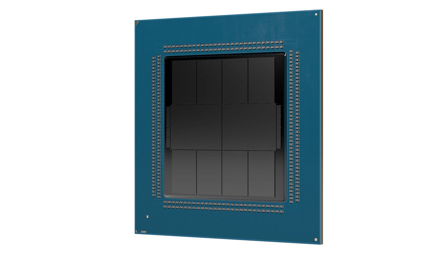
The Venice CPUs, likely utilizing an advanced TSMC 2nm or refined 3nm process node, represent a departure from incrementalism. From a semiconductor perspective, the move to Zen 6 involves a significant increase in Instructions Per Clock (IPC) driven by a redesigned branch predictor and a wider execution engine. However, the most critical innovation for Venice lies in its “L3-heavy” topology.
AMD has recognized that in the 2026 landscape, memory latency and data movement are the primary constraints for hyperscalers. By optimizing the chiplet interconnect—likely through a next-generation Infinity Fabric implementation—Venice minimizes the penalty for cross-CCD (Core Complex Die) communication. This is vital for sovereign AI clouds and massive database management where core-to-core synchronization is constant.
The focus on rack density is also evident; by maintaining a manageable Thermal Design Power (TDP) while pushing core counts beyond the 128-core threshold of previous generations, AMD offers a Total Cost of Ownership (TCO) proposition that challenges Intel’s Clearwater Forest and beyond.
On the accelerator front, the MI400 series, built on the CDNA 4 architecture, is AMD’s answer to the post-Blackwell era. The MI400 moves toward a more modular tile-based design, integrating HBM4 memory to reach bandwidth levels previously reserved for high-end networking fabrics. The architectural leap here is the MI400’s specialized Tensor core units, which are now optimized for a wider array of data types, including FP4 and Microscaling formats.
This flexibility is essential for the 2026 AI market, where Large Language Model (LLM) quantization has become the standard for deployment efficiency.
The synergy between Venice and MI400 cannot be ignored. AMD is leveraging a unified software stack (ROCm 7.x) and a shared hardware-level memory coherency protocol. This allows the Venice CPU to act as a highly efficient host for MI400 clusters, reducing the “CPU bottleneck” often seen in heterogeneous AI training.
For the enterprise, this integrated roadmap signifies that AMD is no longer just providing components; they are providing a holistic “AI factory” blueprint. As we look at the competitive landscape against Nvidia and Intel, AMD’s success will hinge on the yield of these ambitious 2nm designs and the continued maturation of the ROCm ecosystem to rival CUDA’s dominance.