Executive Summary
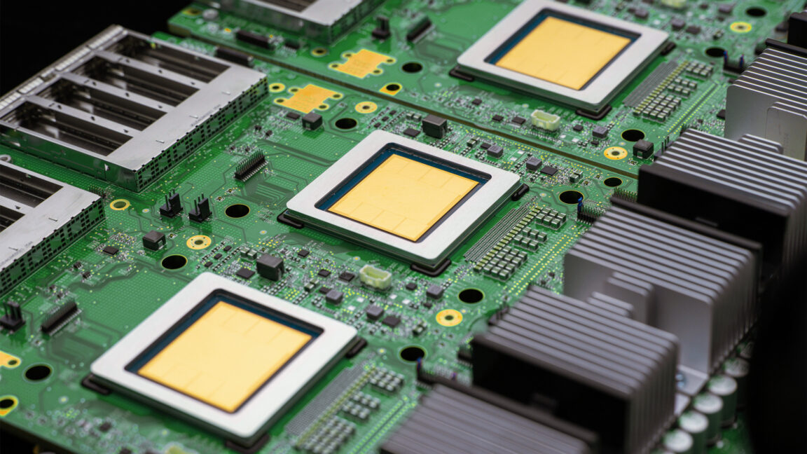
- To meet the unprecedented compute demands of the “agentic era,” Google has unveiled a radical shift in its custom silicon strategy: a dual-TPU system that splits AI processing into two specialized chips. Unlike the unified, general-purpose approach seen in NVIDIA’s H100 or the newer Blackwell B200 architectures, Google’s latest generation of Tensor Processing Units allocates distinct silicon for training and inference. This technical segregation is a strategic response to the unique operational profile of autonomous agents, which require constant, low-latency background reasoning—a task for wh…
Strategic Deep-Dive
To meet the unprecedented compute demands of the “agentic era,” Google has unveiled a radical shift in its custom silicon strategy: a dual-TPU system that splits AI processing into two specialized chips. Unlike the unified, general-purpose approach seen in NVIDIA’s H100 or the newer Blackwell B200 architectures, Google’s latest generation of Tensor Processing Units allocates distinct silicon for training and inference. This technical segregation is a strategic response to the unique operational profile of autonomous agents, which require constant, low-latency background reasoning—a task for which versatile but power-hungry GPUs are increasingly inefficient.
The necessity of this dual-chip architecture stems from the move toward “always-on” agentic workflows. A standard LLM chatbot is transactional; it consumes power only when a user submits a prompt. In contrast, an autonomous agent managing a supply chain or monitoring a network is persistent.
It is constantly ingesting data, performing “background reasoning,” and executing tasks even when no human is present. This persistent compute demand creates a massive inference bottleneck. By deploying a dedicated inference chip optimized for energy efficiency and responsiveness, and a separate training chip optimized for raw throughput and backpropagation, Google can achieve a lower Total Cost of Ownership (TCO) compared to using general-purpose clusters.
In the competitive landscape, this move is a direct challenge to NVIDIA’s market dominance. While NVIDIA’s GPUs are the gold standard for model flexibility, Google’s specialized TPUs offer a more cost-effective path for the “long tail” of agentic deployment. By tailoring silicon to the specific mathematical operations required for agentic inference—such as maintaining long-term memory and context windows—Google can offer GCP (Google Cloud Platform) customers higher performance at a lower cost per token.
This vertical integration—owning the chip, the framework, and the agent platform—creates a powerful ecosystem that is difficult for NVIDIA or even other cloud providers like AWS to replicate without their own specialized silicon.
Furthermore, this hardware evolution addresses the thermal and power constraints of modern data centers. As agent fleets scale to thousands of instances per enterprise, the heat generated by traditional general-purpose chips becomes a physical barrier to deployment. Google’s inference-specific TPU is designed to handle sustained loads with significantly reduced power draw, allowing for denser server rack configurations.
As the industry moves from “training massive models” to “running massive fleets of agents,” the winners will be determined not just by model parameters, but by the efficiency of the underlying silicon. Google’s dual-TPU strategy positions it as the only provider capable of sustaining the compute-intensive reality of the agentic era at scale.


