Executive Summary
- A South Korean court has sentenced a former Samsung Electronics engineer to seven years in prison for orchestrating a massive leak of semiconductor trade secrets to the Chinese firm CXMT. The stolen data encompassed over 600 critical process steps related to 10nm-class DRAM manufacturing, a core pillar of Samsung’s memory dominance. The engineer reportedly received approximately $2 million in exchange for information that could significantly accelerate China’s domestic chip production capabilities.
Strategic Deep-Dive
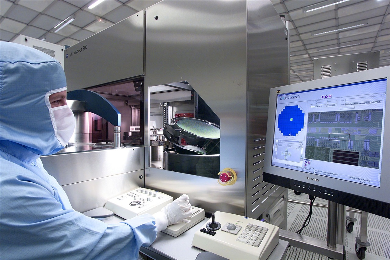
The sentencing of a former Samsung Electronics engineer to seven years in prison marks a watershed moment in South Korea’s legal defense of its technological sovereignty. The defendant was convicted of transferring a comprehensive “turnkey” package of semiconductor manufacturing secrets to ChangXin Memory Technologies (CXMT), a state-backed Chinese firm aggressively pursuing domestic DRAM self-sufficiency. The scale of this intellectual property theft is unprecedented, involving the illicit transfer of over 600 intricate process steps essential for the fabrication of 10nm-class DRAM—a node that currently serves as the “technological moat” for the South Korean memory giant.
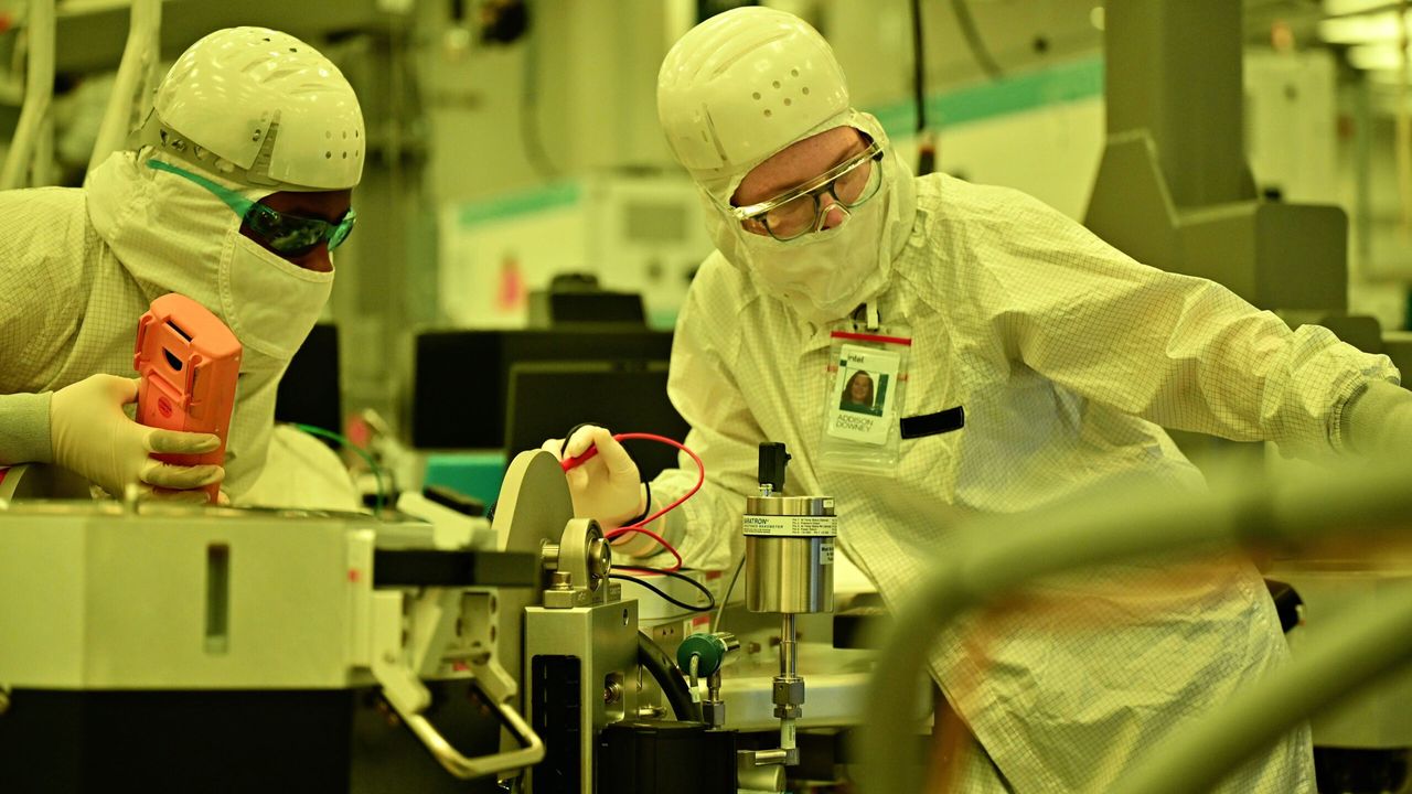
To appreciate the gravity of this breach, one must understand the immense technical complexity of the 10nm DRAM process. At this scale, manufacturing involves Extreme Ultraviolet (EUV) lithography, multi-patterning sequences, and the management of high-aspect-ratio contact (HARC) etching. Each of the 600 process steps represents a meticulously refined variable—from specific chemical vapor deposition (CVD) gas ratios to precise thermal annealing timings.
These are not merely instructions; they are the result of multi-billion dollar R&D cycles and decades of cumulative “tribal knowledge.” By acquiring these 600 steps, CXMT essentially skipped the most painful phases of the learning curve, potentially shaving three to five years off their development timeline for advanced memory products.
The motivation behind the espionage was purely financial, with the defendant reportedly receiving approximately $2 million for the data. This underscores the predatory “talent poaching” strategies utilized by international competitors to bypass Western-led export controls. As the U.S.
and its allies restrict China’s access to high-end EUV equipment, Beijing has prioritized the acquisition of “process know-how” to optimize existing Deep Ultraviolet (DUV) machinery. Samsung’s 10nm secrets provided exactly that: a roadmap for extracting 10nm-level performance from legacy or restricted hardware setups.
The South Korean judiciary’s decision to hand down a seven-year sentence—a term significantly higher than historical averages for industrial theft—reflects a growing consensus that semiconductor secrets are a matter of national economic security. However, for Samsung and the broader “K-Chip” industry, the damage is likely irreversible. Once 600 process steps are integrated into a competitor’s workflow, the technological gap narrows instantly.
As we move into an era of 2nm and 3nm logic and sub-10nm DRAM, the protection of this “process moat” will require more than just legal deterrents; it will necessitate a fundamental overhaul of internal data security and human capital management within the global semiconductor supply chain.