Executive Summary
- TSMC unveils A13 node as direct successor to A14 for next-generation AI compute
Strategic Deep-Dive
TSMC Unveils A13 Node as Direct Successor to A14 for Next-Generation AI Compute
TSMC, AI 연산 혁신을 위한 차세대 A13 공정 공개 및 옹스트롬 시대 선도
KEYWORDS_EN: TSMC, A13, Node Shrink, AI Hardware, Semiconductor Fabrication, A14, Angstrom Era
KEYWORDS_KR: TSMC, A13 공정, 미세 공정, AI 하드웨어, 반도체 파운드리, 옹스트롬, 공정 미세화
ENG_CONTENT
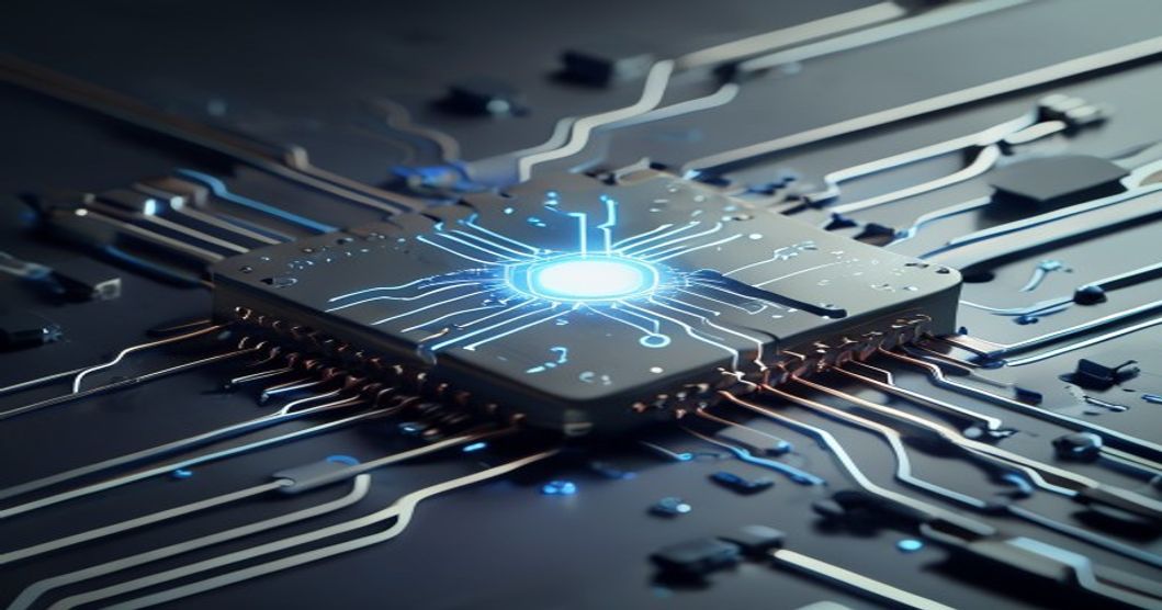
At the 2026 North America Technology Symposium, TSMC officially debuted the A13 process node, a critical addition to its “Angstrom-class” roadmap. Positioned as a direct successor to the A14 node announced last year, the A13 is characterized as a “direct shrink.” In the complex world of semiconductor lithography, a direct shrink is a highly strategic move that optimizes the existing gate-all-around (GAA) transistor architecture to achieve higher density and improved power-performance metrics without the long lead times associated with a completely new platform architecture. This allows lead customers, particularly in the AI accelerator and mobile SoC sectors, to achieve a faster Time-to-Market (TTM) for their next-generation products.
The naming convention itself marks a new phase in the “node war” between TSMC, Intel, and Samsung. With Intel aggressively marketing its 14A node, TSMC’s A13 is a clear tactical response designed to maintain its lead in logic density and power efficiency. While the A14 focused on the initial implementation of advanced backside power delivery, the A13 refines these features to squeeze out additional performance-per-watt gains.
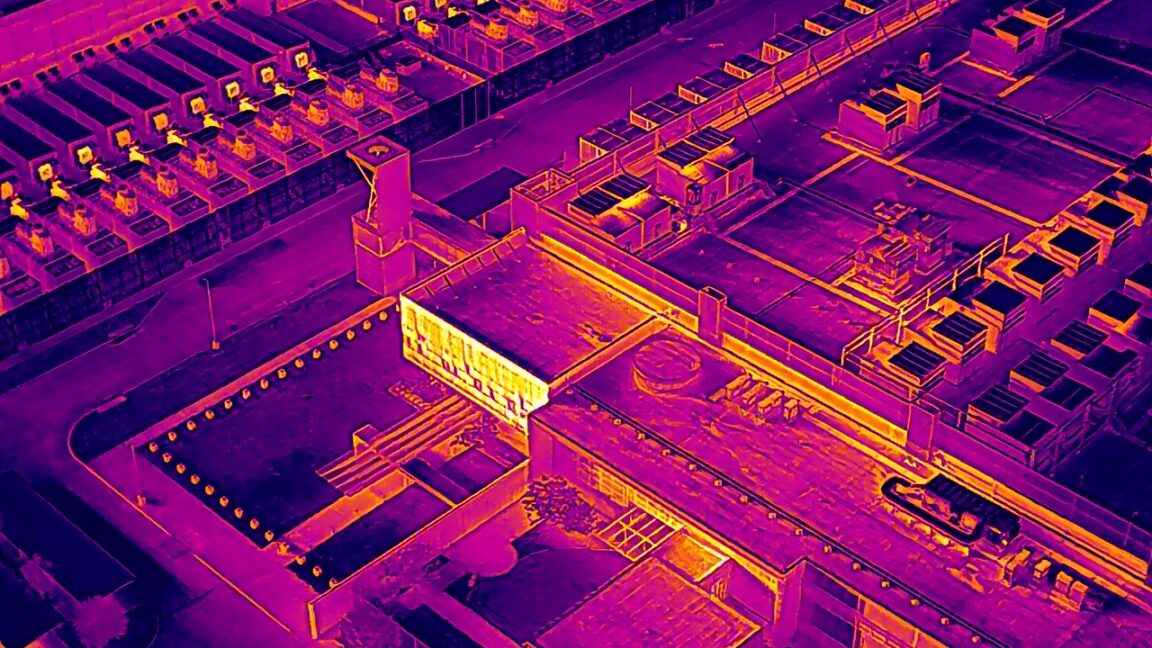
This is crucial because, in 2026, the industry is no longer just fighting for the smallest transistor, but for the best thermal management at the wafer level. As AI chips push 1,000 watts and beyond, any efficiency gain from the fabrication node directly translates into lower cooling costs for the end data center operator.
From a market perspective, the A13 node arrives at a time of “insatiable customer demand.” Hyperscalers are currently engaged in a massive hardware upgrade cycle, moving from 5nm and 3nm designs to 2nm-class (A-series) hardware. The A13 offers a sweet spot in the manufacturing curve; it leverages the yield-learning from the A14 while providing the “compact design” benefits necessary for Edge AI devices where battery life and form factor are paramount. By offering A13 as a refined, high-yield alternative to the earlier A14, TSMC ensures that its N2/N3 capacity transitions smoothly into the A-series era without the production bottlenecks that sometimes plague first-generation nodes.
Technically, the A13 node is expected to feature advanced packaging compatibility, specifically targeting CoWoS (Chip-on-Wafer-on-Substrate) and SoIC (System-on-Integrated-Chips) technologies. This integration is vital for the upcoming 2027 generation of AI accelerators that will require tighter integration between logic and HBM4. TSMC’s mastery of both the frontend fabrication (A13) and the backend advanced packaging allows it to offer a turnkey solution that rivals find difficult to match.
As we look at the competitive landscape, the A13 reinforces TSMC’s status as the “foundry of choice” for the world’s most sophisticated AI workloads.
KOR_CONTENT
Technical Definition of the Next-Generation A13 Process and the Dawn of the Angstrom Era
TSMC has officially unveiled its next-generation A13 process at the 2026 North America Technology Symposium. Positioned as a “Direct Shrink” version of the A14 node announced last year, the A13 is characterized by its sophisticated Angstrom-class architecture that maximizes device density and power efficiency. Beyond simply reducing circuit linewidth, this strategic choice by TSMC aims to secure the stability of the GAA (Gate-All-Around) transistor structure and provide customers with opportunities for faster Time-to-Market.
Competition with Intel 14A and the Value of Process Miniaturization
Amidst the intensifying competition for node naming in the semiconductor industry, TSMC’s A13 is expected to be a powerful weapon against Intel’s 14A process. A13 particularly refines the Backside Power Delivery technology, significantly improving performance per watt. By addressing the greatest challenge currently facing AI semiconductors in 2026, the issue of heat generation, at the process level, it is expected to perfectly meet the needs of global hyperscalers looking to reduce data center operating costs.
Optimized Solutions for AI and Edge Computing
The A13 process simultaneously targets the explosive demand for AI computation and the improvement of edge AI performance in mobile devices. TSMC applies the yield know-how accumulated from A14 to A13 to increase production stability while optimizing the combination with advanced packaging technologies such as CoWoS and SoIC. This enables next-generation AI accelerator and high-performance workstation chipset manufacturers to design smaller, more powerful hardware.
TSMC is expected to once again demonstrate its overwhelming technological advantage in the foundry market through A13, solidifying its position as the number one market share leader.
IMAGE_PROMPT: A macro shot of a sophisticated 2nm-class silicon wafer with intricate circuitry glowing in electric blue, featuring the TSMC logo in a high-tech cleanroom environment.
ORIGINAL_URL: https://www.techpowerup.com/img/GPZCLcxCd1f8wcke.jpg