Executive Summary
- Silicon Valley startup Bolt Graphics has achieved a major milestone with the successful tape-out of its Zeus GPU on the TSMC 12nm node. By transitioning from FPGA emulation to hardened silicon, the company promises a 17-fold reduction in compute costs through architectural optimization, challenging the dominance of high-cost cutting-edge nodes with mature-process efficiency.
Strategic Deep-Dive
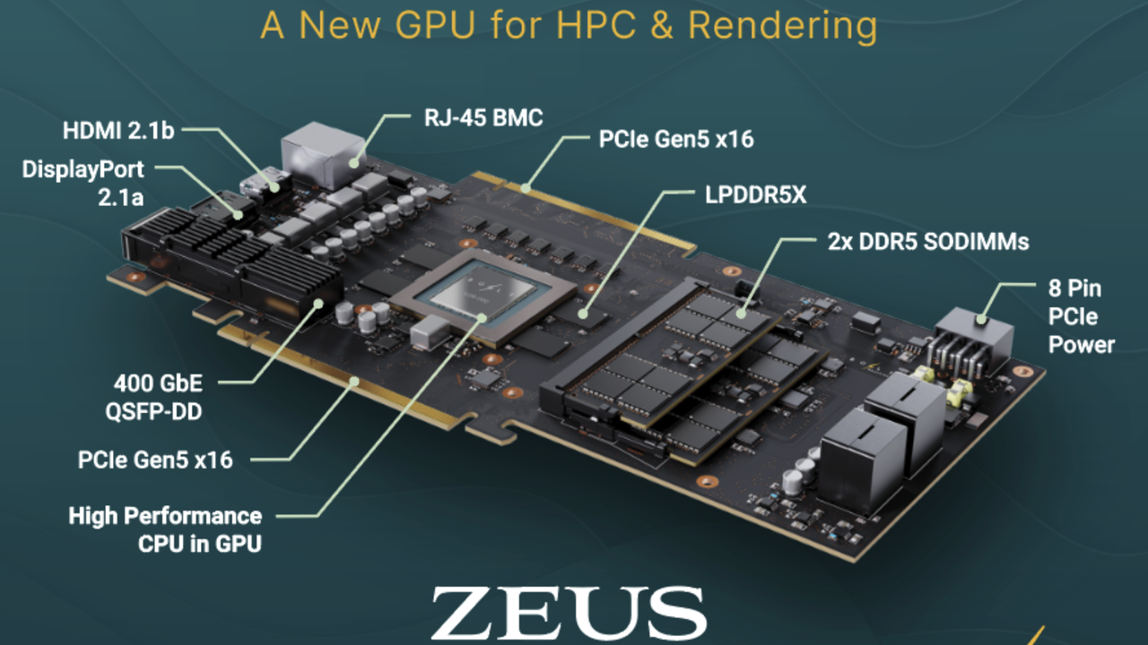
Bolt Graphics, an emerging force in semiconductor design, has announced the successful tape-out of its inaugural Zeus GPU, utilizing TSMC’s well-established 12nm process node. This transition from software-defined FPGA emulation to physical silicon marks a watershed moment for the startup, moving it closer to commercializing an architecture that claims to reduce the cost of compute by a factor of 17. As a Senior Semiconductor Analyst, I find the choice of the 12nm node particularly compelling.
While the rest of the industry is locked in an economically grueling race toward 3nm and 2nm, Bolt Graphics is leveraging the stability and high yields of a mature node to deliver a specialized compute engine that prioritizes throughput efficiency over raw transistor density.
The technical significance of the Zeus GPU lies in its architectural departure from general-purpose GPU (GPGPU) designs. By hardening specific AI and graphics math functions into the silicon—moving away from the overhead inherent in FPGA structures—Bolt Graphics has managed to eliminate significant power-delivery network (PDN) inefficiencies and reduce intra-chip communication latencies. This ’lean architecture’ approach allows the Zeus GPU to punch significantly above its weight class.
From a data architect’s perspective, the 17x reduction in compute cost is likely achieved by optimizing the memory-to-logic ratio and utilizing non-traditional data pathways that minimize the energy required for data movement, which is the primary cost driver in modern AI workloads.
For the broader industry, Bolt Graphics serves as a case study in ‘Architectural Scaling’ versus ‘Process Scaling.’ By proving that a 12nm design can compete on a cost-per-inference basis with chips manufactured on far more expensive nodes, Bolt Graphics is challenging the inevitability of the soaring prices for AI hardware. This has profound implications for startups and research institutions that have been priced out of the current Nvidia-dominated market. The successful tape-out signals that the first physical samples are imminent, and the industry will be watching the ensuing benchmarks with intense interest.
If the 17x efficiency claim holds true under real-world workloads, Bolt Graphics could effectively commoditize high-performance AI compute, shifting the market focus from who has the smallest transistors to who has the most intelligent hardware architecture. This is a bold gamble on the idea that in the era of mass-scale AI deployment, the most cost-effective silicon will ultimately dictate the winner.