Executive Summary
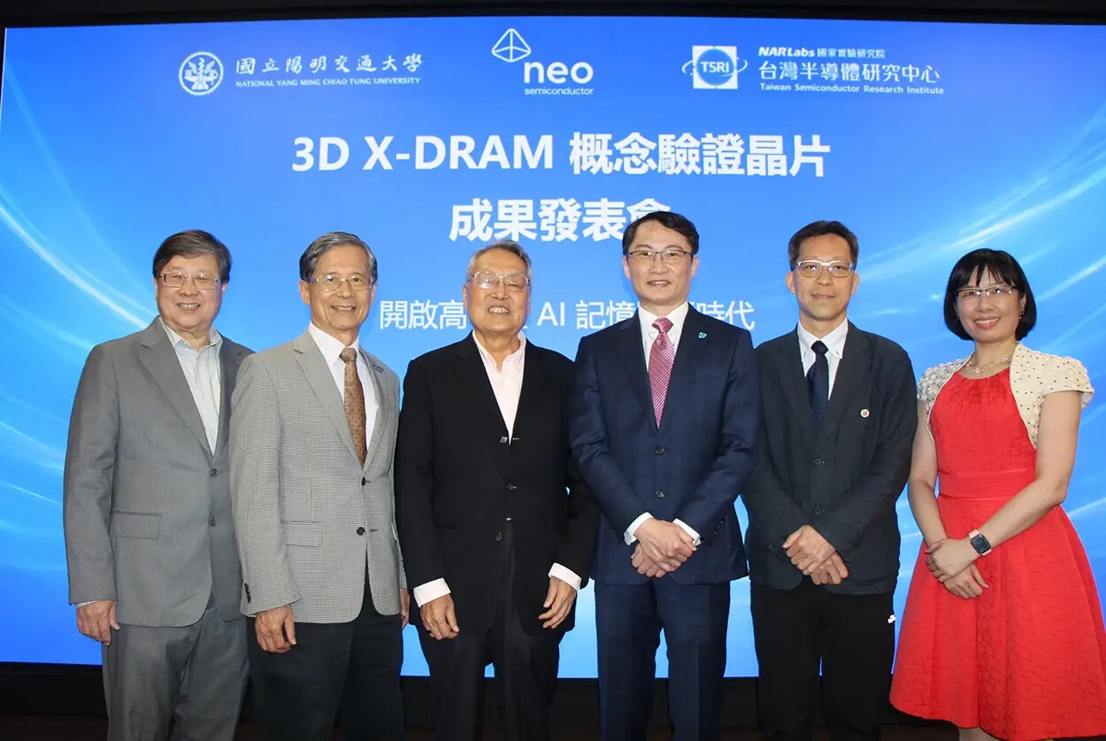
- NEO Semiconductor has marked a historic milestone in the memory industry by successfully demonstrating the Proof-of-Concept (POC) for its proprietary 3D X-DRAM technology. This breakthrough addresses the critical scaling bottlenecks of traditional DRAM by leveraging vertical stacking architectures. In a major show of industry confidence, the company also secured a strategic investment led by Stan Shih, the legendary founder of Acer, positioning NEO as a primary contender in the high-density memory market required for the next generation of AI-centric computing systems.
Strategic Deep-Dive
NEO Semiconductor’s announcement regarding the successful Proof-of-Concept (POC) for its 3D X-DRAM represents a fundamental shift in how the industry approaches memory scaling. For decades, the semiconductor world has struggled with the planar limitations of DRAM, where traditional lithographic shrinking has reached a point of diminishing returns. By applying a vertical integration strategy—similar to the architectural evolution that allowed NAND flash to achieve terabit densities—NEO Semiconductor is offering a viable roadmap for the high-performance, high-density memory that is absolutely essential for the AI era.
The successful POC validates that the 3D X-DRAM architecture can maintain the necessary speed and reliability of DRAM while exponentially increasing capacity within the same physical footprint.
The strategic weight of this development is further amplified by the high-profile investment led by Stan Shih, the founder and former Chairman and CEO of Acer. Shih’s involvement is far more than a simple capital injection; it is a profound endorsement from a pioneer who helped build the modern global PC and semiconductor supply chain. For a disruptive startup like NEO Semiconductor, having a figure of Shih’s stature provide strategic guidance and financial backing is a signal to major foundries and hyperscalers that 3D X-DRAM is ready for the transition from conceptual research to commercial implementation.
This backing effectively lowers the perceived risk for future partners and customers who are looking for the next big leap in memory technology to support massive Large Language Models (LLMs).
From a technical perspective, 3D X-DRAM solves the ‘memory wall’ problem that currently bottlenecks AI hardware. While High Bandwidth Memory (HBM) focuses on the throughput between the GPU and the memory, 3D X-DRAM targets the raw density and power efficiency required for local processing and massive data storage tiers. By utilizing a floating body cell structure that eliminates the need for complex capacitors, NEO’s design simplifies the manufacturing process compared to current sub-10nm DRAM attempts.
This simplification, combined with the vertical stacking, suggests a path toward drastically lower costs per bit, which is the primary metric for data-centric infrastructure. As we move toward 2027 and beyond, the ability of companies like NEO Semiconductor to bridge the gap between lab-proven concepts and high-volume manufacturing will define the competitive landscape of AI hardware. The successful POC and the strategic alignment with industry titans like Stan Shih position NEO not just as an innovator, but as a potential standard-setter for the next decade of memory evolution.
The industry is now watching closely to see how NEO integrates this technology into the existing semiconductor ecosystem and whether it can catalyze a shift away from the expensive and complex traditional DRAM scaling roadmap.