Executive Summary
- Intel has reached a watershed moment in its high-stakes journey to regain semiconductor manufacturing leadership, reporting tangible progress in its most advanced process nodes. The company’s 18A process node, which represents the pinnacle of its current technological roadmap, is seeing meaningful yield improvements. This development is critical for the semiconductor industry, as yield stability is the primary metric used by fabless customers to assess the viability of a foundry partner. Intel’s success in stabilizing 18A yields suggests that the company is on track to deliver high-volume manu…
Strategic Deep-Dive
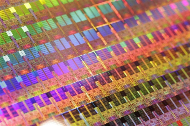
Intel has reached a watershed moment in its high-stakes journey to regain semiconductor manufacturing leadership, reporting tangible progress in its most advanced process nodes. The company’s 18A process node, which represents the pinnacle of its current technological roadmap, is seeing meaningful yield improvements. This development is critical for the semiconductor industry, as yield stability is the primary metric used by fabless customers to assess the viability of a foundry partner.
Intel’s success in stabilizing 18A yields suggests that the company is on track to deliver high-volume manufacturing (HVM) capabilities that could challenge the current market hierarchy.
Design Enablement: The Strategic Leap from PDK 0.5 to 0.9
Simultaneously, Intel is aggressively pushing forward with its 14A (1.4nm-class) process node, which has now reached the ’early design enablement’ stage. The release of the 0.5 Process Design Kit (PDK) for 14A marks the official start of customer engagement for this next-generation node. A PDK is a collection of software tools and data used by chip designers to ensure their architectures are compatible with a specific fabrication process.
By providing the 0.5 version, Intel is allowing early-adopter customers to begin preliminary floorplanning and architectural modeling.
Management has underscored that the next critical milestone is the transition to the 0.9 PDK. This transition is far from a mere administrative update; it represents a major leap in process maturity, offering near-final design rules and performance parameters. For a senior data analyst, the move from 0.5 to 0.9 is the most high-risk yet high-reward phase of design enablement, as it requires the synchronization of electronic design automation (EDA) tools with real-world silicon performance.
Intel’s ability to meet its PDK 0.9 schedule will be the ultimate litmus test for its 14A readiness.
Reclaiming the Foundry Crown
Intel’s dual-track success—stabilizing 18A while enabling 14A—is reshaping the competitive narrative in the foundry sector. In an era where AI-specific silicon requires the most advanced lithography and packaging techniques, Intel is positioning itself as a legitimate alternative to established incumbents. The company’s focus on design enablement ensures that it isn’t just building factories, but is fostering an ecosystem where external customers can innovate with confidence.
By engaging customers at the PDK 0.5 stage, Intel is effectively locking in long-term partnerships that will span the remainder of the decade. As the company moves toward the 0.9 PDK milestone, the industry will be watching closely to see if Intel can deliver on its promise of process parity and eventual leadership. These milestones are not just technical achievements; they are the foundation of Intel’s future as a global foundry powerhouse.


