Executive Summary
- The semiconductor landscape is witnessing a historic realignment as SK Hynix and TSMC formalize an expansive partnership centered on the development and integration of HBM4 technology. Announced at the TSMC North America Technology Symposium 2026, this collaboration marks a strategic pivot toward ‘Memory-Logic Integration,’ a paradigm shift designed to meet the extreme demands of next-generation AI accelerators. As a Lead Data Architect, I view this partnership as the industry’s most robust response to the ‘Memory Wall’—the physical and architectural limitation where data transfer speeds betwe…
Strategic Deep-Dive
The semiconductor landscape is witnessing a historic realignment as SK Hynix and TSMC formalize an expansive partnership centered on the development and integration of HBM4 technology. Announced at the TSMC North America Technology Symposium 2026, this collaboration marks a strategic pivot toward ‘Memory-Logic Integration,’ a paradigm shift designed to meet the extreme demands of next-generation AI accelerators. As a Lead Data Architect, I view this partnership as the industry’s most robust response to the ‘Memory Wall’—the physical and architectural limitation where data transfer speeds between the processor and memory cannot keep pace with computational power.
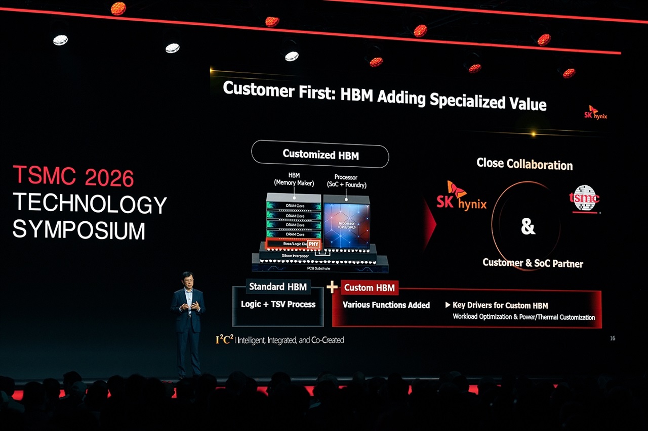
HBM4 is the technological vanguard of this movement, featuring a groundbreaking 2048-bit interface that doubles the bus width compared to HBM3e. The synergy here is profound: for the first time, the base die of the HBM stack will be manufactured using TSMC’s advanced logic processes (likely 7nm or 5nm) rather than traditional memory processes. This allows for the integration of complex logic functions directly into the memory stack, enabling features like hybrid bonding that significantly increase TSV (Through-Silicon Via) density and improve thermal management.
For Large Language Model (LLM) inference, where memory bandwidth is the primary performance constraint, this integration promises a quantum leap in throughput. Beyond the technical specs, the SK Hynix-TSMC alliance is a calculated ‘Anti-Samsung’ maneuver. By uniting the world’s leading pure-play foundry with the market leader in high-bandwidth memory, the duo provides a formidable alternative to Samsung’s integrated device manufacturing (IDM) model.
This partnership offers hyperscalers like Nvidia, Google, and Amazon a more flexible, ‘best-of-breed’ approach to silicon design. While Samsung leverages its internal coordination to offer a one-stop shop, the SK Hynix-TSMC alliance leverages specialized expertise to push the envelope of 3D packaging and CoWoS (Chip on Wafer on Substrate) technology. This collaborative model ensures that the HBM4 interface becomes the de facto standard for the high-performance computing (HPC) market.
As AI models move toward trillions of parameters, the ability to fuse logic and memory into a single, cohesive unit will be the defining characteristic of the winners in the 2026-2030 semiconductor cycle. The SK Hynix-TSMC nexus is not just a supply agreement; it is a vision of a unified silicon architecture that will power the next decade of artificial intelligence.