Executive Summary
- SoftBank’s subsidiary SaiMemory is collaborating with Intel to develop Z-Angle Memory (ZAM), a radical low-power alternative to HBM for AI workloads, backed by Japanese government funding.
Strategic Deep-Dive
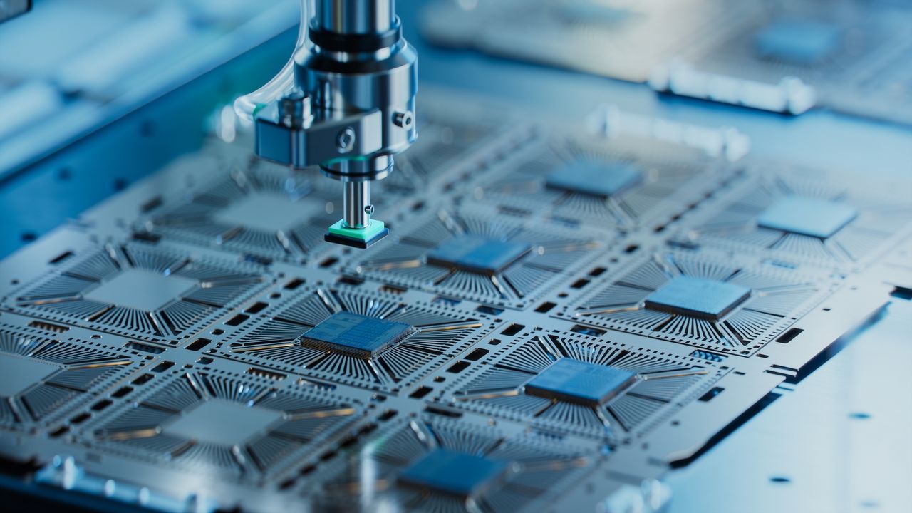
In a strategic maneuver to redefine the landscape of AI infrastructure, SaiMemory—a key subsidiary of the Japanese tech giant SoftBank—has entered into a high-stakes collaborative partnership with Intel. This alliance focuses on the R&D and eventual mass production of Z-Angle Memory (ZAM), a radical new DRAM architecture designed as a direct technical response to the escalating power and thermal challenges posed by current High Bandwidth Memory (HBM) standards. As Large Language Models (LLMs) grow in complexity, the industry has encountered a physical wall; the energy required to move data between the processor and HBM is becoming a dominant portion of the total system power envelope.
ZAM is being engineered to provide a viable low-power alternative that sustains HBM-like performance without the prohibitive thermal throttling associated with traditional vertical stacked solutions.
The project’s significance is amplified by the official procurement of financial subsidies from Japan’s New Energy and Industrial Technology Development Organization (NEDO). This government backing underscores the profound geopolitical dimensions of the contemporary semiconductor race. Rather than merely expanding existing manufacturing capacity, Japan is pivoting toward funding localized Research and Development that targets future-critical IP.
By fostering a domestic champion in SaiMemory and pairing it with the technical prowess of Intel’s engineering teams, Tokyo aims to secure a pivotal and sovereign position in the global AI hardware supply chain. For Intel, this provides a necessary vector to integrate next-generation memory technology closer to its logic tiles, potentially creating a highly efficient integrated computing platform that bypasses the limitations of standard DDR or current HBM interposers.
Technically, ZAM represents a fundamental departure from the current industry reliance on 3D Through-Silicon Vias (TSV). While specific details on the ‘Z-Angle’ geometry are classified, market analysts speculate that it utilizes an angular or hybrid bonding approach to optimize signal paths, thereby reducing parasitic capacitance and power leakage. This shift toward workload-specialized memory arrives at a critical juncture where hyperscalers are desperate for hardware that can manage the spiraling operational costs of AI.
If successful, ZAM could disrupt the market duopoly currently enjoyed by SK Hynix and Micron, offering a more sustainable and cost-effective scaling path for the next decade of AI development. The localized nature of this R&D also highlights a broader global trend: nations are no longer content to import standard commodities; they are funding the fundamental science to ensure they own the underlying architectural intellectual property of the silicon era.