Executive Summary
- NEO Semiconductor has successfully completed proof-of-concept testing for its 3D X-DRAM, utilizing established 3D NAND processes to offer a high-performance, lower-cost alternative to HBM for AI workloads.
Strategic Deep-Dive
Breaking the HBM Monopoly with 3D X-DRAM
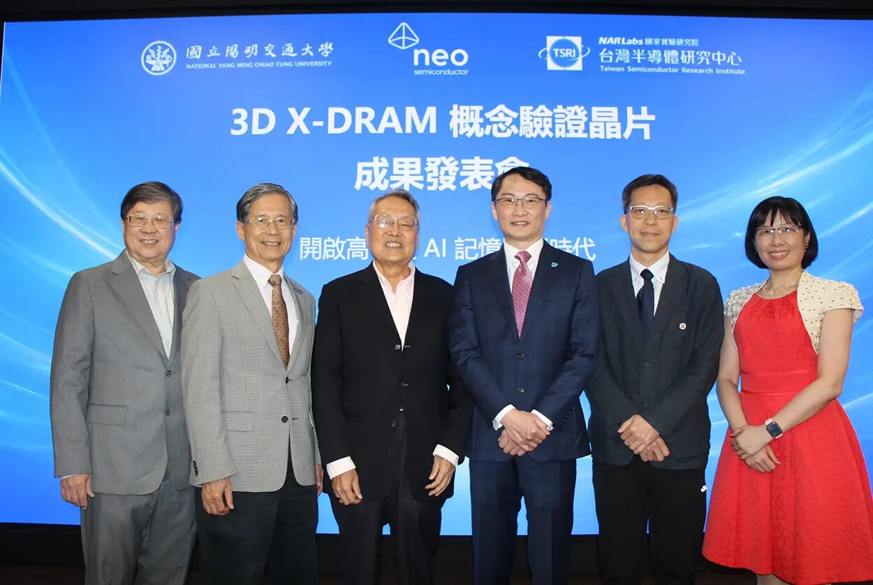
NEO Semiconductor has reached a critical milestone in the memory industry by announcing the successful proof-of-concept (PoC) validation of its 3D X-DRAM technology. As the demand for high-performance AI processors continues to surge, the industry has been plagued by the high costs and manufacturing complexities of High Bandwidth Memory (HBM). NEO Semiconductor’s 3D X-DRAM aims to disrupt this landscape by providing a high-capacity, high-speed memory solution that addresses the current economic and supply-side bottlenecks in AI infrastructure.
By demonstrating that DRAM can be structured using advanced vertical architectures, the company is opening a new path for scaling memory density without the astronomical price tags associated with current top-tier AI memory solutions.
Technical Granularity: Leveraging Proven 3D NAND Processes
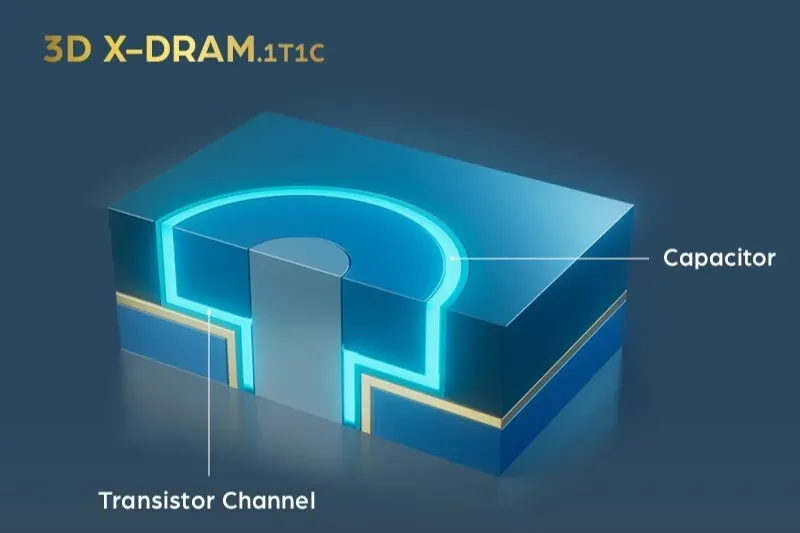
The technical brilliance of 3D X-DRAM lies in its strategic utilization of established 3D NAND manufacturing processes. To understand the cost advantage, one must look at the structural differences: HBM relies on Through-Silicon Via (TSV) technology and complex micro-bump bonding to stack multiple DRAM dies. This process requires extreme precision, specialized equipment, and results in lower yields and high thermal management costs.
In contrast, 3D X-DRAM adapts the ‘staircase etching’ and ‘channel hole’ technologies used in 3D NAND flash memory. These techniques are already mature and optimized for high-volume manufacturing. By applying these vertical stacking methods to DRAM, NEO Semiconductor can achieve superior density and bandwidth while utilizing existing fabrication workflows and lithography equipment.
This approach significantly lowers the barrier to entry and allows for mass production at a fraction of the capital expenditure required for traditional HBM expansion.
Strategic Funding and Market Entry
Following the successful PoC, the company has secured significant new funding to accelerate the development of this next-generation memory. This capital injection will be used to refine the 3D X-DRAM architecture, focusing on reducing latency and increasing the data transfer rates to compete directly with HBM3 and HBM4 specifications. By positioning 3D X-DRAM as a cost-effective alternative for AI servers and data centers, NEO Semiconductor is challenging the dominance of major incumbents like Samsung and SK Hynix.
As the industry moves toward more diverse AI hardware ecosystems, the ability to provide affordable, scalable memory will be the defining factor in which technologies gain long-term market traction.