Executive Summary
- SMIC is recalibrating its long-term roadmap by shifting focus from front-end wafer fabrication to advanced backend packaging technologies.
- The foundry is aggressively scaling internal R&D teams dedicated to high-performance computing (HPC) and sophisticated chiplet architectures.
- This strategic move aims to bypass international lithography restrictions by maximizing system-level performance through integration innovation.
Strategic Deep-Dive
SMIC, China’s largest and most advanced foundry, is undergoing a profound strategic metamorphosis as it navigates the increasingly restrictive global semiconductor landscape. Traditionally, SMIC has focused its capital and R&D on advancing its front-end wafer fabrication nodes to close the gap with industry leaders like TSMC and Samsung. However, the current geopolitical climate—characterized by stringent U.S.
export controls on Extreme Ultraviolet (EUV) lithography and advanced Deep Ultraviolet (DUV) equipment—has forced a tactical retreat from pure-play node shrinking. In response, SMIC is aggressively pivoting toward advanced packaging as its primary engine for growth in the AI and high-performance computing (HPC) sectors. This shift is marked by a massive scaling of internal specialized teams and a significant reallocation of capital expenditure toward backend integration technologies.
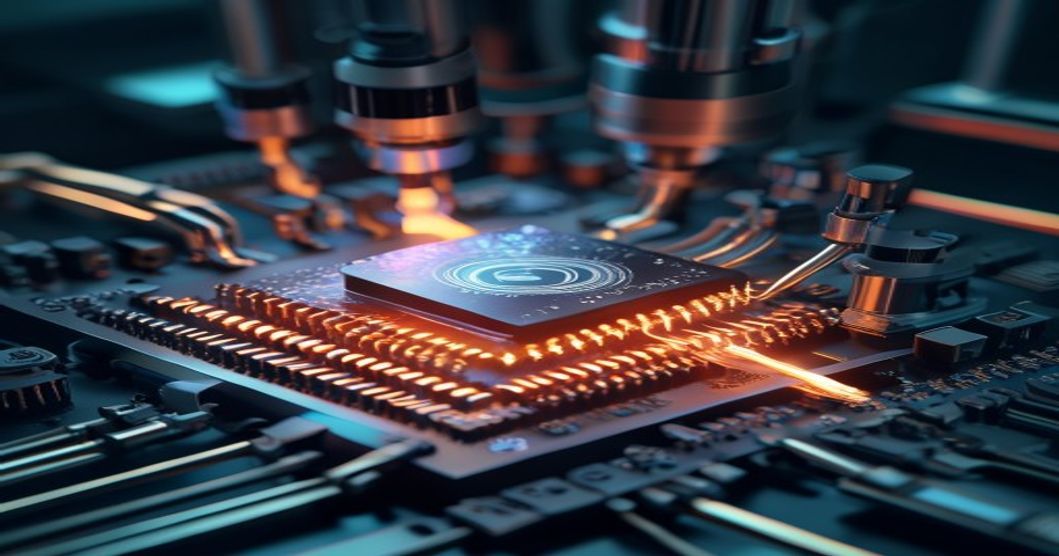
Advanced packaging, particularly 2.5D, 3D, and Chiplet-based architectures, offers a viable pathway to enhance system-level performance without relying solely on the latest nanometer-scale transistors. By integrating multiple functional tiles into a single package, SMIC aims to deliver the compute density required for large-scale AI training and inference. This approach acknowledges that the ‘More than Moore’ era provides a unique opportunity for foundries with limited lithography access to remain competitive through architectural innovation.
The scaling of these internal teams suggests that SMIC no longer views packaging as a commodity backend service but as a high-value, strategic pillar of its AI chip roadmap. Furthermore, this move aligns with China’s broader national goal of achieving semiconductor self-sufficiency. By mastering complex interconnect technologies and thermal management solutions, SMIC positions itself as the critical hub for domestic high-performance silicon designers who are similarly locked out of global leading-edge foundries.
As SMIC builds out this ecosystem, the success of its advanced packaging initiative will determine whether China can maintain its momentum in the global AI race despite significant manufacturing headwinds. The focus is now on throughput (처리량) and interconnect density rather than just gate pitch, signaling a new chapter in SMIC’s technical evolution.