Executive Summary
- Silicon IP leader M31 has achieved a critical milestone by completing the tapeout of its eUSB2V2 interface IP on TSMC’s N2P (2nm) manufacturing platform. This accomplishment confirms the readiness of the 2nm ecosystem, offering fabless companies a validated path to exploit the power and performance gains of the Nanosheet-based N2P node for high-performance computing and mobile applications.
Strategic Deep-Dive
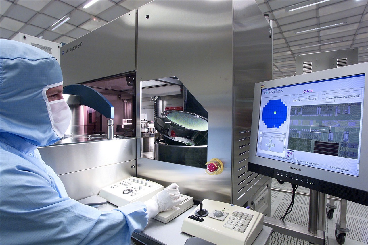
The semiconductor industry is currently navigating the complex transition toward the 2nm era, a shift characterized by the move from traditional FinFET structures to Nanosheet (Gate-All-Around) transistors. In this high-stakes environment, the synergy between independent IP providers and foundries has become the primary determinant of ecosystem maturity. M31, a premier silicon intellectual property provider, has announced the successful tapeout of its eUSB2V2 interface IP on TSMC’s N2P (2nm) manufacturing platform.
This milestone is not merely a technical achievement; it represents a critical strategic alignment required for the next generation of high-performance computing (HPC) and advanced mobile hardware.
The N2P Node: A New Paradigm in Performance
TSMC’s N2P node is the apex of the company’s 2nm family, introducing significant advancements in power delivery and transistor density. Unlike the preceding N3 node, N2P leverages Nanosheet technology to provide a substantial leap in Power, Performance, and Area (PPA). However, the complexity of this node presents immense challenges for signal integrity and parasitic capacitance management.
M31’s eUSB2V2 IP addresses these issues by integrating specialized circuit architectures tailored to the unique physical properties of the N2P platform. The eUSB2V2 standard is essential for low-voltage, high-speed data transfers in AI-driven mobile devices and data centers. By completing the tapeout, M31 has proven that its silicon IP can handle the rigorous demands of 2nm lithography while maintaining operational stability.
Overcoming Gating Factors for Fabless Adoption
For global fabless giants, the primary gating factor for migrating to a sub-3nm node is the availability of silicon-proven IP. Without a robust library of foundation and interface IPs, the risk of design failure increases exponentially, potentially leading to catastrophic losses in Capital Expenditure (Capex). Scott Chang, CEO of M31, emphasized that the 2nm landscape requires IP to be developed in tandem with the fabrication process itself.
This ‘deep integration’ ensures that predictive models for silicon behavior are highly accurate, reducing the need for costly and time-consuming redesign cycles. The eUSB2V2 tapeout provides a ‘plug-and-play’ assurance for chip designers, effectively lowering the barrier to entry for the N2P node and ensuring that the industry can maintain its rapid time-to-market pace in 2026.
Strategic Market Implications
As we look toward the 2026 product cycles, M31’s early success on the N2P node strengthens TSMC’s competitive moat against rival foundries. It establishes a high-performance ecosystem where hardware innovators can immediately leverage the benefits of 2nm scaling. From an analyst’s perspective, the readiness of critical interface IPs like eUSB2V2 is a leading indicator of a node’s commercial viability.
As TSMC prepares for volume production, the existence of a verified IP portfolio will accelerate the migration of AI accelerators and premium application processors to the 2nm stage. M31’s achievement serves as a technical benchmark, signaling that the building blocks for the next decade of advanced computing are now solidified. The focus now shifts to yield optimization and the expansion of the IP library to include other high-speed standards on the N2P platform.