Executive Summary
- As AI data centers hit the physical limits of copper-based interconnects, the industry is witnessing a massive architectural shift toward high-fidelity optical modules to eliminate throughput bottlenecks and maintain scaling laws.
Strategic Deep-Dive
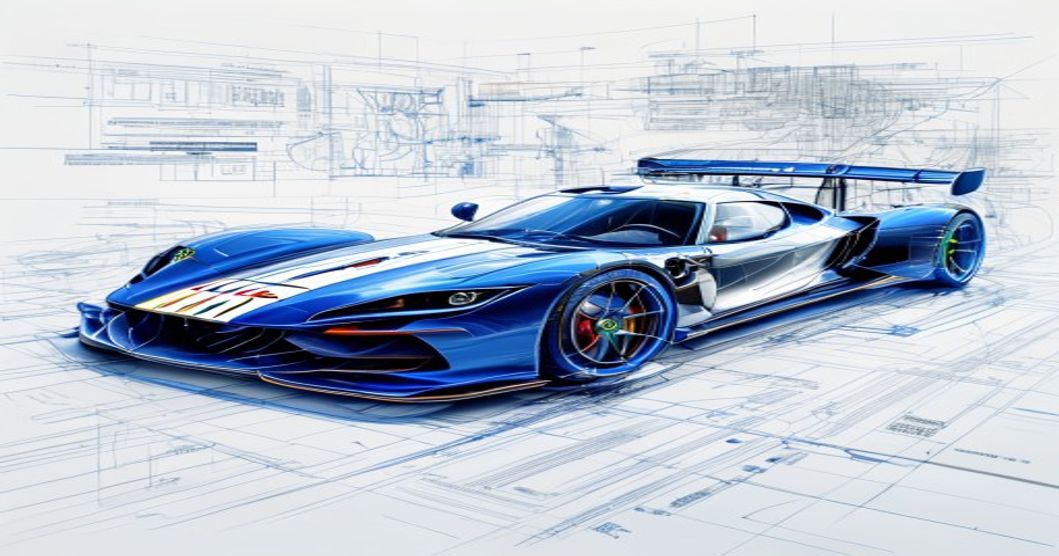
The artificial intelligence sector is currently navigating a fundamental architectural crisis: the ‘Interconnect Wall.’ For the past several years, the race was defined by the raw FLOPs (Floating Point Operations per Second) generated by silicon. However, as we scale toward giant model training clusters, the primary inhibitor of performance is no longer the individual processing unit, but the latency and bandwidth of the fabrics that connect them. This shift is driving an unprecedented surge in demand for high-end optical modules, as data center architects realize that without a high-fidelity networking fabric, expensive GPU clusters remain drastically underutilized due to I/O wait states.
Technically, we are witnessing the obsolescence of traditional copper-based electrical interconnects at the rack scale. As signal frequencies increase to support higher throughput, copper suffers from severe signal attenuation and thermal dissipation issues. At the speeds required for next-generation AI—approaching 1.6T and 3.2T per port—the physical properties of electrons in copper traces simply cannot maintain the required signal integrity without prohibitive power consumption.
This has necessitated the rapid adoption of optical interconnects. Optical modules, which convert electrical signals into light and back again, offer near-zero latency cycles and massive bandwidth-distance products that electrical wires cannot match. The market’s bullish reaction to optical stocks is a direct reflection of this hardware necessity; the industry is effectively rewiring the brain of the modern data center.
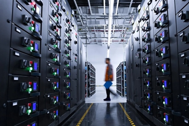
From a systems engineering perspective, the focus is now on reducing the power overhead of these conversions. The current industry standard utilizes pluggable optical transceivers, but the roadmap is aggressively pivoting toward Co-Packaged Optics (CPO). By moving the optical engine onto the same substrate as the switch silicon or the GPU, architects can eliminate long electrical traces, reducing power consumption by up to 30% and significantly improving thermal envelopes.
This is vital because power density in AI racks is already pushing the limits of liquid cooling technologies. The move from pluggable to CPO represents a major shift in the semiconductor assembly and test (OSAT) supply chain, as traditional networking and chip packaging merge into a singular, complex discipline.
Furthermore, the transition from PCIe Gen 5 to Gen 6 and the imminent Gen 7 has accelerated this trend. Each leap in generation doubles the bandwidth, but it also exponentially increases the challenge of signal integrity. Retimers and redrivers can only do so much; eventually, the only way to maintain the necessary throughput across the scale of a massive data center is to go optical as close to the silicon as possible.
This ‘Optical-First’ architecture is the new gold standard for AI hardware. As we move through 2026, the strategic importance of optical module manufacturers—and the specialty foundries that produce their photonic integrated circuits (PICs)—will only grow. The bottleneck has been identified, and the solution is light-based communication, marking the end of the copper era in high-performance computing.