Executive Summary
- ASML is aggressively flattening its organizational structure to boost execution speed as it navigates a strategic standoff with TSMC over the economic feasibility and timing of High-NA EUV integration.
Strategic Deep-Dive
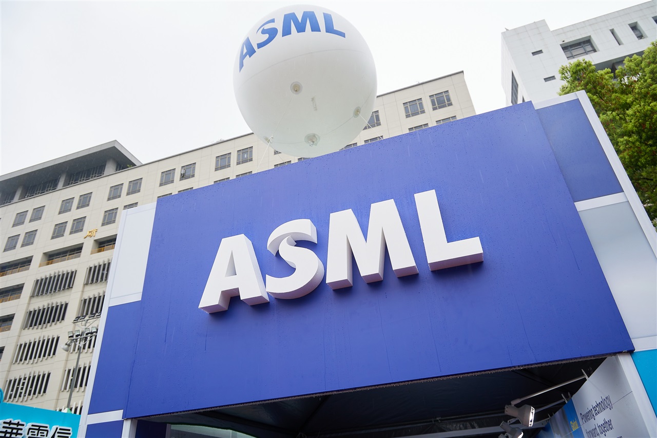
ASML, the lynchpin of the global semiconductor supply chain, is currently executing a significant internal transformation characterized by the elimination of multiple management layers. According to internal communications reviewed by Business Insider, the company is moving toward a flatter organizational structure to streamline execution and accelerate decision-making cycles. While such moves are common in struggling firms, for a monopoly-status company like ASML, it signals a proactive defense against organizational inertia at a critical technological juncture: the rollout of High-NA (0.55 Numerical Aperture) EUV lithography.
The strategic context of this restructuring is deeply intertwined with the skepticism voiced by its primary customer, TSMC. While ASML is pushing the industry toward sub-2nm nodes with High-NA EUV, TSMC has remained uncharacteristically cautious, citing the ’economic threshold’ of the new systems. The friction arises from a fundamental disagreement on the cost-benefit analysis of the equipment, which carries a price tag exceeding $350 million per unit.
TSMC argues that the increase in lithographic pitch precision and the reduction in multi-patterning steps may not justify the capital expenditure (CapEx) burden if yields do not improve exponentially. In response, ASML’s management flattening is an attempt to become more lean and responsive, potentially to better align its engineering roadmap with the economic realities faced by foundry leaders.
From an architectural standpoint, the transition to High-NA EUV is not just about a larger lens; it involves a complete rethink of the photoresist chemistry and mask technology. The organizational complexity within ASML had reached a point where internal silos were hindering the rapid feedback loops required to solve these multi-disciplinary challenges. By removing management bloat, ASML aims to empower its lead architects to work more directly with client-facing support teams.
This is a crucial pivot as the industry moves toward ‘Hyper-NA’ concepts in the long term, where the margin for error in lithographic alignment is measured in picometers. ASML is effectively preparing for a future where its dominance is challenged not by a competitor, but by the economic limits of Moore’s Law.
Furthermore, the timing of this restructuring suggests that ASML is bracing for a period of intensified strategic maneuvering. As TSMC signals a possible delay in High-NA adoption for its first-wave 2nm production, ASML must maintain its financial health while continuing heavy R&D investment. The management cuts are a clear signal to shareholders that the company is prioritizing operational excellence over administrative expansion.
This lean approach is designed to ensure that ASML remains agile enough to pivot its resources toward Intel or Samsung if they decide to use High-NA as a ’leapfrog’ opportunity to close the gap with TSMC. Ultimately, the success of ASML’s flatter organization will be measured by its ability to drive down the total cost of ownership for its tools, making the move to sub-10nm logic not just a physical possibility, but a financial inevitability for the entire industry.