Executive Summary
- Samsung Electronics has reportedly achieved a technological breakthrough with sub-10nm DRAM production, while SK Hynix prepares to sample HBM4E, intensifying the race for memory density and AI-optimized bandwidth.
Strategic Deep-Dive
The semiconductor memory sector is currently witnessing a dual-track revolution that challenges the fundamental limits of solid-state physics. According to industry insiders and reports from The Elec, Samsung Electronics has successfully produced a ‘working die’ for sub-10nm DRAM. This achievement is a critical indicator that the physical scaling of DRAM, which many experts predicted would plateau at the 10nm barrier due to capacitor leakage and interference issues, has a viable path forward.
The successful fabrication of a functional sub-10nm die suggests that Samsung has mastered the integration of High-K metal gates (HKMG) and potentially new vertical transistor architectures to maintain cell capacitance at a scale where traditional materials fail. This breakthrough allows for a higher transistor density within the same silicon footprint, directly translating to increased capacity and lower power-per-bit for next-generation data centers.
Simultaneously, SK Hynix is doubling down on its dominance in the AI memory space. The company is reportedly entering the sampling phase for HBM4E, the next evolution in its high-bandwidth memory portfolio. As AI models scale from billions to trillions of parameters, the bandwidth requirements for memory-to-processor communication have become the primary bottleneck in throughput.
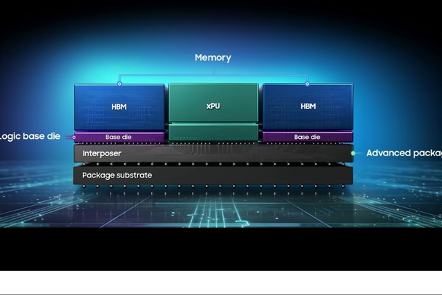
HBM4E is expected to introduce even more aggressive vertical stacking, utilizing advanced TSV (Through-Silicon Via) techniques and potential hybrid bonding to reduce the thickness of the memory stack while increasing the interconnect density. By sampling HBM4E ahead of the broader market, SK Hynix is positioning itself to be the sole supplier for the next wave of ‘super-chips’ that integrate compute and memory into a single, cohesive package. The integration of a logic-based base die in HBM4E is a particularly notable architectural pivot, as it allows for on-memory processing of basic data functions, reducing the load on the main GPU/NPU.
From a data architect’s perspective, these developments represent a pincer movement in hardware design. Samsung’s sub-10nm DRAM provides the foundation for massive, low-power system memory (DDR6/LPDDR6), while SK Hynix’s HBM4E provides the high-octane fuel for specialized AI accelerators. The material science hurdles in sub-10nm—specifically the lithographic pitch and the aspect ratio of the capacitor towers—require a level of precision that only a few foundries globally can achieve.
Samsung’s ability to produce a working die at this node is a signal to the market that it remains at the absolute cutting edge of manufacturing technology, countering recent narratives of falling behind in the HBM race.
As we look toward 2027, the synergy between these two memory advancements will define the capabilities of the global tech stack. The transition to sub-10nm nodes will necessitate a shift in power management ICs (PMICs) and thermal solutions at the system level, as the power density of these ultra-dense chips creates new cooling challenges. Meanwhile, the HBM4E sampling by SK Hynix will likely accelerate the development of ultra-high-scale AI clusters, where thousands of these memory stacks operate in parallel.
This is a high-stakes engineering battle where the winner dictates the performance floor for all future computing hardware. The rivalry between Samsung’s manufacturing-centric scaling and SK Hynix’s architecture-centric scaling is the primary engine driving the next generation of the global hardware economy.