🔍 Executive Summary
- The HCL-Foxconn joint venture has secured Taiwan’s CTCI Corporation as its EPC lead to architect a foundational OSAT facility in Uttar Pradesh, marking a pivotal advancement in India's semiconductor manufacturing sovereignty and back-end ecosystem.
Strategic Deep-Dive
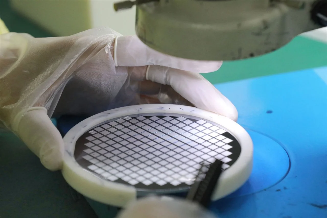
The strategic alignment between the HCL-Foxconn joint venture and Taiwan’s CTCI Corporation signifies a major structural shift in the global semiconductor landscape. As a Senior Data Systems Architect, it is clear that the development of an Outsourced Semiconductor Assembly and Testing (OSAT) facility in Uttar Pradesh is not merely an industrial expansion but a complex engineering feat that requires specialized infrastructure capable of supporting high-density interconnects and advanced packaging technologies. CTCI, as the EPC partner, brings critical expertise in constructing high-tech environments that must adhere to stringent ISO cleanroom standards.
For OSAT operations to be viable, the facility must incorporate vibration-isolated flooring systems to protect sensitive flip-chip and wire-bonding equipment from seismic and mechanical interference. Furthermore, the architecture requires robust ultra-pure water (UPW) systems and specialized chemical delivery networks, which are essential for the cleaning and etching processes inherent in modern semiconductor packaging. The choice of CTCI underscores the joint venture’s commitment to mimicking the high-yield manufacturing environments found in Hsinchu or Kaohsiung.
From a systems perspective, the facility will integrate advanced Power Management Systems (PMS) to ensure 24/7 operational continuity, a non-negotiable requirement for semiconductor processes where power fluctuations can lead to catastrophic yield losses. This project is a cornerstone of the ‘Semiconductor India’ initiative, aiming to fill the void in the domestic electronics value chain. Currently, India possesses strong design capabilities but lacks the physical back-end infrastructure to support a complete ‘design-to-market’ cycle.
By establishing this OSAT hub, the HCL-Foxconn JV is creating a localized node that can service both domestic demand and international export markets, effectively reducing lead times and logistical overheads. Moreover, the collaboration facilitates a technology transfer between Taiwan’s mature engineering sector and India’s growing industrial base. The technical challenges of setting up such a facility in Uttar Pradesh involve navigating local utility constraints; however, the involvement of a firm like CTCI, experienced in international large-scale EPC projects, mitigates these risks.
This move also highlights the increasing importance of System-in-Package (SiP) and heterogeneous integration in the AI era. As chips become more complex, the packaging layer becomes the primary driver of performance and thermal efficiency. Therefore, the infrastructure being built today in India is being designed with future scalability in mind, allowing for the eventual integration of advanced 2.5D and 3D packaging technologies.
This foresight ensures that the Indian semiconductor ecosystem remains competitive for the next decade of hardware innovation.