🔍 Executive Summary
- TSMC is aggressively expanding its 3nm capacity to meet surging AI chip demand, creating a formidable market barrier that threatens Samsung's ambitions to leapfrog with its 2nm GAA technology.
Strategic Deep-Dive
Iterative Dominance: TSMC’s 3nm Scale-up
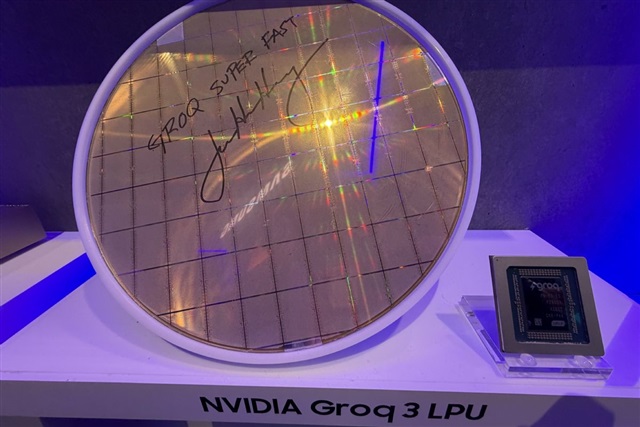
As the global AI buildout reaches a fever pitch, TSMC is leveraging its operational excellence to cement its 3nm dominance. According to a recent analysis by DIGITIMES Insight, TSMC is significantly increasing its capital expenditure to expand the capacity of its N3 (3nm-class) nodes, including the refined N3E and N3P variants. This aggressive expansion is strategically timed to absorb the lion’s share of orders from hyperscalers and AI silicon designers like Nvidia and Apple.
By offering a massive, stable volume of chips based on the mature FinFET architecture, TSMC creates a high-reliability environment that effectively ’locks in’ clients. This ‘capacity-first’ strategy acts as a powerful deterrent to competitors, as the sheer scale of TSMC’s operations allows it to optimize costs and yields at a rate that younger, less utilized nodes cannot match.
Samsung’s GAA Gamble and the Yield Barrier
Samsung Electronics has pursued a fundamentally different path, betting on the Gate-All-Around (GAA) transistor structure starting from its 3nm node. The goal was to leapfrog TSMC by offering superior power, performance, and area (PPA) metrics at the 2nm stage. However, the transition to GAA represents a radical shift in electronic design automation (EDA) tools and IP libraries.
For a fabless company to switch from TSMC’s 3nm FinFET to Samsung’s 2nm GAA, it must undergo a costly and time-consuming redesign process. Currently, many chipmakers are choosing to stick with TSMC’s iterative 3nm improvements because the technical gains offered by Samsung’s early GAA do not yet outweigh the risks of lower yields and supply chain uncertainty. TSMC’s strategy of ‘good enough’ technology delivered at an ‘unmatchable scale’ is proving to be a superior business model in the AI era, where time-to-market is the most critical metric.
CAPEX Disparity and the Future of Foundry Competition
The capital expenditure (CAPEX) disparity between TSMC and its rivals has become a structural barrier to entry. TSMC’s ability to invest tens of billions of dollars annually into capacity expansion—backed by its massive cash reserves—ensures that it can meet the insatiable silicon hunger of the AI sector. While Samsung and Intel are striving to prove their 2nm and 1.8A capabilities, they face the ‘chicken-and-egg’ problem: without a massive anchor tenant (like Apple or Nvidia), they cannot fund the scale required to match TSMC’s cost efficiency.
Furthermore, TSMC is integrating advanced packaging solutions like CoWoS and SoIC directly into its 3nm/2nm workflow, creating a ‘one-stop-shop’ that Samsung’s foundry division is still struggling to replicate at scale. As long as TSMC maintains this lead in both capacity and packaging, the ’leapfrogging’ strategy of rivals remains a theoretical possibility rather than a market reality, leaving Samsung’s 2nm ambitions on the back foot as it fights to secure even a fraction of the high-end AI market.