🔍 Executive Summary
- TSMC has unveiled a groundbreaking CoWoS roadmap through 2029, aiming for a 48x compute increase and a 34x bandwidth jump. The plan centers on massive 14-reticle size packages capable of integrating 24 HBM5E stacks, signaling a shift from traditional node shrinking to system-level scaling.
Strategic Deep-Dive
The semiconductor industry is witnessing a fundamental shift from monolithic die scaling to system-level integration, and TSMC’s latest CoWoS (Chip on Wafer on Substrate) roadmap is the definitive blueprint for this transition. By 2029, TSMC anticipates that advanced packaging innovations will deliver a staggering 48-fold increase in computational power and a 34-fold leap in memory bandwidth compared to today’s state-of-the-art AI accelerators. This trajectory is not merely ambitious; it is a calculated response to the physical and economic limits of traditional node shrinking below 2nm.
The centerpiece of this roadmap is the transition to massive-scale packaging. TSMC aims to produce interposers that exceed 14 times the size of a standard photolithography reticle. To put this in perspective, the industry is currently moving toward 3.3x reticle sizes (CoWoS-L).
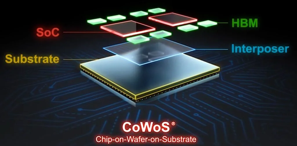
Expanding to 14x requires solving immense challenges in silicon interposer yield and structural integrity. At this scale, the package becomes a ‘system-on-wafer’ entity, capable of housing dozens of high-performance logic chiplets alongside up to 24 stacks of HBM5E (High Bandwidth Memory). The integration of 24 HBM5E stacks represents a critical milestone for AI workloads, as the growing parameters of Large Language Models (LLMs) demand near-instantaneous access to massive pools of data.
However, housing such dense compute power in a 14-reticle enclosure introduces unprecedented thermal and power delivery hurdles. TSMC is addressing these through the advancement of its SoIC (System on Integrated Chips) platform, specifically focusing on hybrid bonding techniques that eliminate traditional micro-bumps to reduce interconnect resistance and heat generation. We expect to see the adoption of advanced liquid-cooling manifolds integrated directly into the interposer or the use of diamond-based heat spreaders to manage the localized hotspots created by 24 HBM stacks.
From an analyst’s perspective, this roadmap cements ‘Advanced Packaging’ as the primary engine for sustaining Moore’s Law. As the cost per transistor at the leading edge begins to flatten, the economic value shifts toward how effectively these transistors can be interconnected. TSMC’s strategy moves the industry toward a modular, ‘LEGO-like’ architecture where disparate dies—CPU, GPU, NPU, and I/O—are bonded with nanometer precision.
For hyperscalers and AI chip designers like NVIDIA, AMD, and Broadcom, TSMC’s 2029 vision provides a predictable scaling path for the next generation of autonomous AI agents and trillion-parameter models. By breaking the reticle limit, TSMC is effectively decoupling performance growth from the physical constraints of single-die manufacturing, ensuring that the infrastructure for the AI era continues to scale exponentially.