🔍 Executive Summary
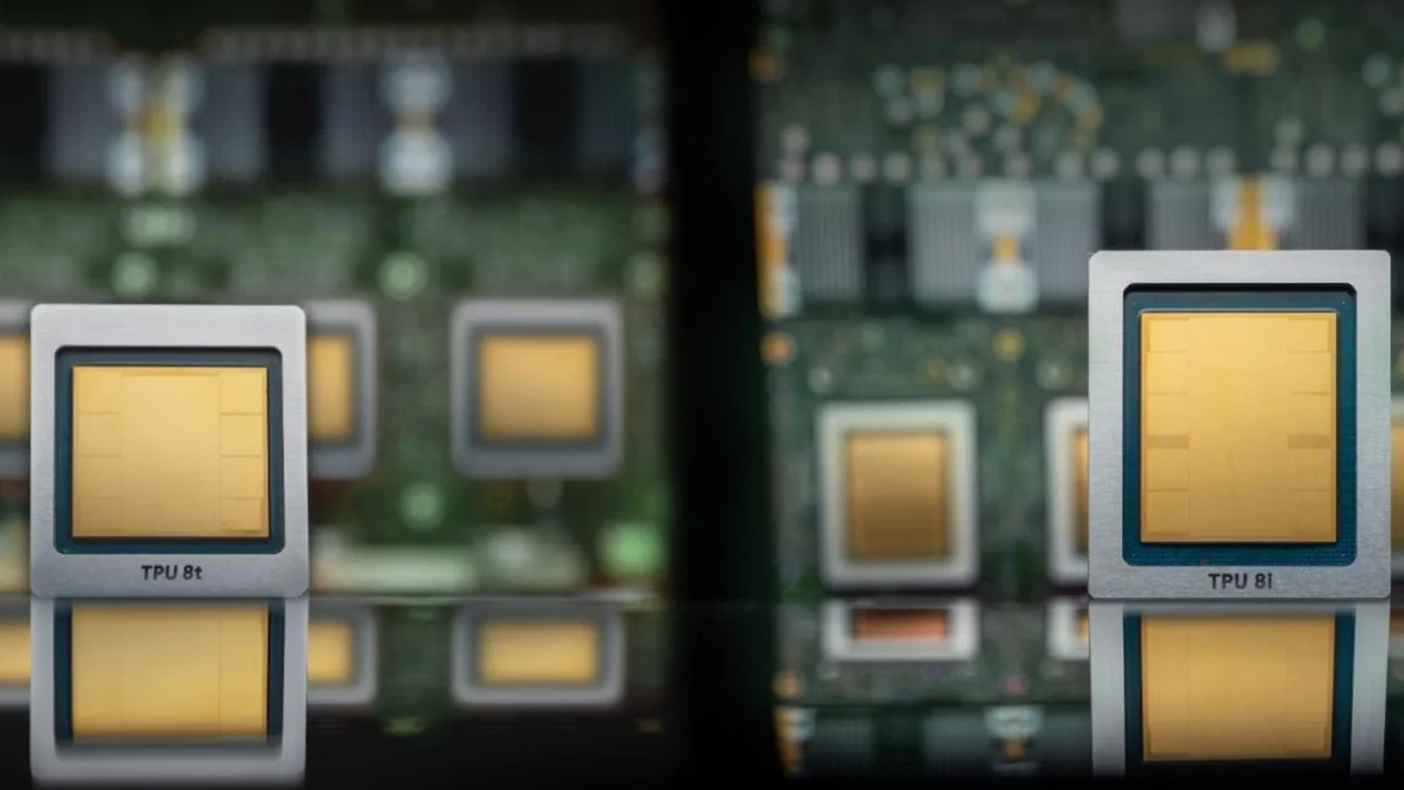
- Google has signaled a paradigm shift in AI silicon with the announcement of the TPU v8. For the first time since the program's inception a decade ago, Google is departing from a unified design to introduce specialized variants for training and inference. This move addresses the diversifying demands of the AI lifecycle, where training requires massive throughput and inference demands extreme efficiency and low latency.
Strategic Deep-Dive
Google has signaled a paradigm shift in AI silicon with the announcement of the TPU v8. For the first time since the program’s inception a decade ago, Google is departing from a unified design to introduce specialized variants for training and inference. This move addresses the diversifying demands of the AI lifecycle, where training requires massive throughput and inference demands extreme efficiency and low latency.
Technical Highlights of the TPU v8 Expansion
- Dual-Chip Architecture: By separating training and inference logic, Google can optimize die area and power delivery for specific instruction sets, avoiding the ‘jack-of-all-trades’ tax found in general-purpose GPUs.
- Unprecedented Networking: The capability to scale up to 1 million nodes per cluster positions Google ahead of traditional data center architectures. This massive parallelism is facilitated by Google’s proprietary optical interconnects, bypassing the bandwidth limitations that often throttle Nvidia-based clusters.
- Vertical Integration: This strategy allows Google to tailor its hardware specifically for its own software stacks, such as the Gemini and Vertex AI ecosystems.
This evolutionary step suggests that Google views the ‘system-as-a-computer’—the cluster itself—as the primary competitive unit, rather than the individual chip. By mastering the network fabric, Google maintains a strategic advantage in deploying the world’s largest AI models at a lower cost-per-inference than competitors reliant on off-the-shelf GPU hardware.