🔍 Executive Summary
- Kyocera Corporation is addressing the most persistent bottleneck in high-performance computing—advanced packaging—with its new Multilayer Ceramic Core Substrate. As AI data centers scale to handle massive xPUs and switch ASICs, the limitations of traditional organic substrates, particularly regarding thermal expansion and structural integrity, have become a primary concern for chip designers.
Strategic Deep-Dive
Kyocera Corporation is addressing the most persistent bottleneck in high-performance computing—advanced packaging—with its new Multilayer Ceramic Core Substrate. As AI data centers scale to handle massive xPUs and switch ASICs, the limitations of traditional organic substrates, particularly regarding thermal expansion and structural integrity, have become a primary concern for chip designers.
Overcoming Material Science Hurdles
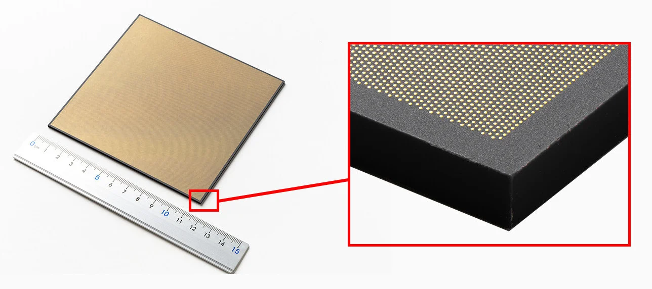
- Coefficient of Thermal Expansion (CTE): Ceramics offer a CTE much closer to silicon than organic materials, reducing mechanical stress during the intense thermal cycling of AI workloads. This ensures flatness and connection reliability even in ultra-large package sizes.
- Signal Integrity at High Frequencies: Ceramic materials possess superior dielectric properties, allowing for cleaner high-speed signaling across the substrate—a requirement for the next generation of data center switch ASICs.
- Thermal Management: The inherent thermal conductivity of Kyocera’s ceramic core facilitates more efficient heat dissipation from the die to the cooling solution, allowing for higher clock speeds and increased power density.
Scheduled for a full unveiling at ECTC 2026, Kyocera’s ceramic solution represents a strategic shift in the industry. As we reach the physical limits of organic substrates, material science at the base level is becoming as vital as the silicon nodes themselves. By reclaiming the role of ceramics in advanced packaging, Kyocera is providing the structural foundation necessary for the next decade of AI hardware scaling.


