🔍 Executive Summary
- In a historic leap for semiconductor manufacturing, Samsung Electronics has reportedly developed the world's first single-digit nanometer-class (10a) DRAM working die. This breakthrough represents the successful navigation of the '10nm barrier,' utilizing functional prototypes to stabilize extreme ultraviolet (EUV) lithography conditions and accelerate the path toward high-yield mass production.
Strategic Deep-Dive
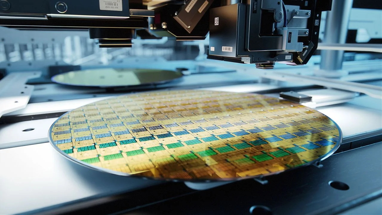
Samsung Electronics has achieved a monumental milestone in semiconductor fabrication by successfully developing the world’s first working die for single-digit nanometer-class (10a) DRAM. This accomplishment marks the formal breaching of the ‘10nm barrier,’ a psychological and physical threshold that has loomed over the memory industry for years. In the lexicon of semiconductor manufacturing, a ‘working die’ is a functional prototype that proves the viability of a new node before it moves into high-volume manufacturing (HVM).
By securing this die, Samsung has demonstrated that its path toward sub-10nm memory is not just theoretical, but functionally sound.
The transition to the 10a node is fraught with immense technical challenges, primarily centered around signal stability and electrical leakage. As the feature size shrinks into the single digits, the dielectric layers and capacitors within the DRAM cell must be engineered with atomic-level precision to prevent parasitic capacitance and data corruption. Samsung has leveraged its extensive experience with multi-layer Extreme Ultraviolet (EUV) lithography to reach this stage.
The company is currently using the 10a prototypes to conduct rigorous fine-tuning of its process conditions. This phase is critical for identifying potential defects early and optimizing the yield curve—the speed at which a new node reaches profitable production levels.
The strategic implications of 10a DRAM are vast. In an era where AI workloads demand ever-higher memory density and lower power profiles, the 10a node offers a superior performance-per-watt ratio compared to existing 10nm-class nodes (such as 1b or 1c). For data center operators managing tens of thousands of servers, the power savings afforded by a single-digit nanometer memory chip can translate into millions of dollars in reduced energy costs annually.
Furthermore, this breakthrough provides Samsung with a critical advantage in the High Bandwidth Memory (HBM) market. As HBM4 specifications begin to take shape, the ability to utilize 10a-class dies for the base logic and core memory layers will allow for significantly more bandwidth and capacity within the same thermal envelope.
While rivals like SK Hynix and Micron are also aggressively pursuing their own sub-10nm roadmaps, Samsung’s report of a successful working die suggests it is leading the timeline for yield stabilization. The ‘Super-Gap’ strategy, a cornerstone of Samsung’s corporate identity, is clearly in full effect here. The industry’s attention now shifts to the transition from prototype to mass production, which is expected to occur throughout late 2026 and 2027.
If Samsung can maintain this lead, it will likely capture the lion’s share of the premium AI memory market, setting the standard for the next decade of silicon evolution.