🔍 Executive Summary
- As AI chips transition to sub-3nm nodes and complex heterogeneous integration, the demand for high-end MEMS-based probe cards is surging, positioning the testing infrastructure as a critical value-add in the semiconductor supply chain.
Strategic Deep-Dive
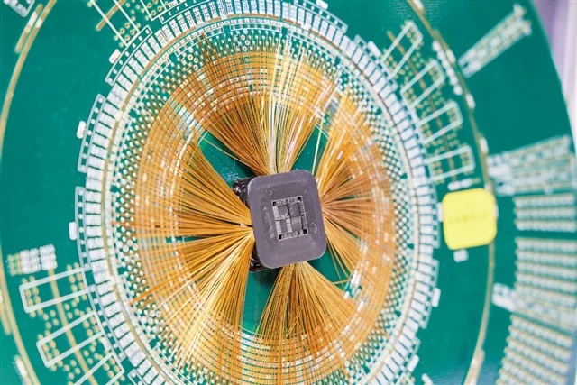
The semiconductor testing landscape is currently undergoing a paradigm shift, driven by the insatiable demand for AI silicon and the resulting migration toward sub-3nm process nodes and heterogeneous integration. As AI accelerators evolve from monolithic designs to complex chiplet-based architectures featuring integrated HBM3e (High Bandwidth Memory), the industry is encountering a massive surge in testing complexity. This evolution has elevated the role of the probe card—a critical electromechanical interface that connects the wafer to Automated Test Equipment (ATE)—from a peripheral consumable to a strategic asset.
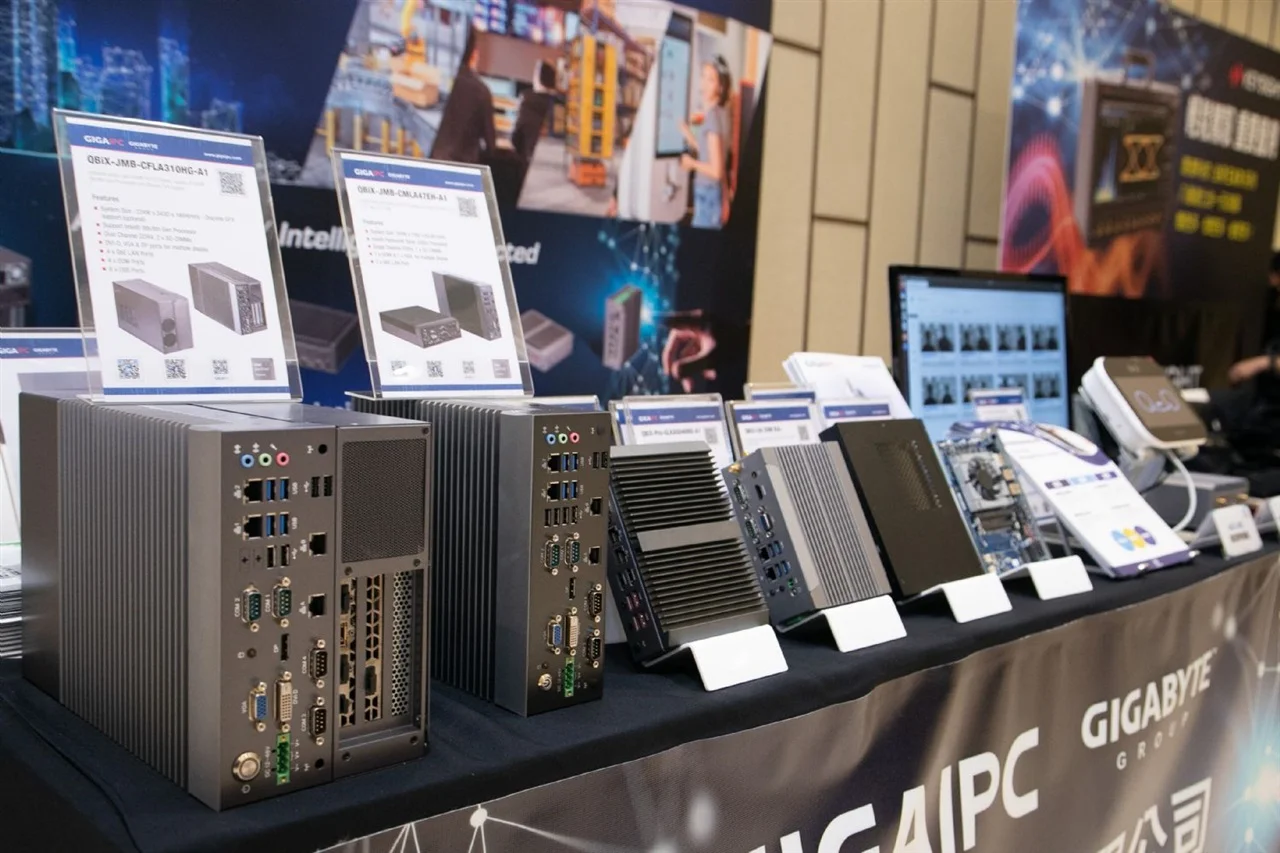
The shift is particularly evident in the transition from traditional cantilever-style probe cards to high-density, MEMS-based (Micro-Electro-Mechanical Systems) vertical probe cards, which are essential for handling the massive pin counts and high-speed signal integrity required by modern AI processors.
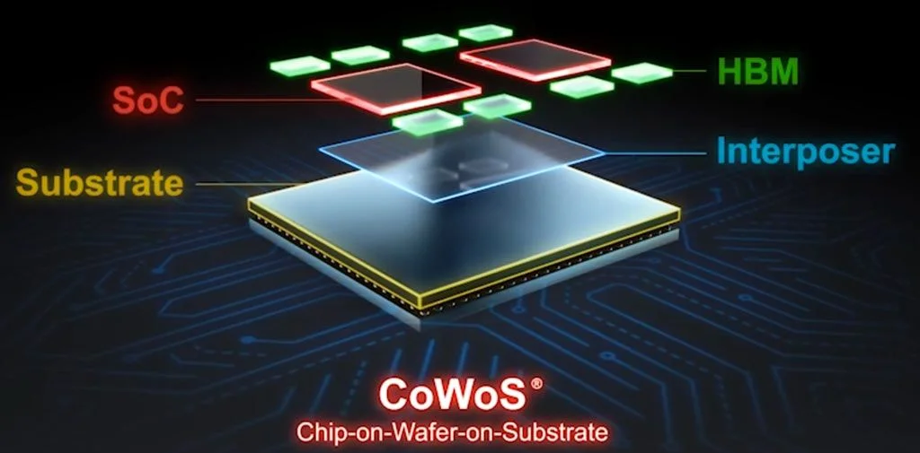
The technical driver behind this surge is the imperative of the ‘Known Good Die’ (KGD) strategy. In an era where 2.5D and 3D packaging technologies like TSMC’s CoWoS (Chip on Wafer on Substrate) or Intel’s Foveros are becoming standard, the cost of a failure during the final assembly stage is catastrophic. If a single defective logic die or a flawed HBM stack is integrated into a multi-chip module, the entire high-value package becomes scrap.
To mitigate this risk, semiconductor manufacturers are implementing far more rigorous and multi-stage testing protocols earlier in the manufacturing flow. This necessitates probe cards with higher durability, advanced thermal management capabilities to handle the immense heat generated by AI chips during power-on tests, and the ability to test thousands of contact points simultaneously without damaging the delicate bumps on the wafer.
Consequently, the upstream supply chain for testing—including materials for probe pins, specialized ceramic substrates, and high-precision testing software—is seeing a significant lift in demand. Industry data suggests that the testing portion of the total semiconductor manufacturing cost is increasing as a percentage of the bill of materials (BOM), reflecting the growing sophistication of the hardware. For OSAT providers and foundries, the ability to deliver high-yield testing services is no longer a given; it is a competitive differentiator.
As HBM3e integration becomes more prevalent in the upcoming generation of B200 or MI300 series chips, the testing requirements will only intensify, requiring further innovations in MEMS probe card manufacturing. This expansion of the testing sector illustrates a broader trend in the industry: as Moore’s Law becomes more difficult and expensive to maintain through lithography alone, the ‘back-end’ of the process—packaging and testing—is becoming the new frontier for value creation and yield preservation. Investors and analysts now view the probe card and testing equipment sector as a leading indicator of the overall health and growth trajectory of the AI hardware ecosystem, signaling that the next major bottleneck in the AI race may not be the fab itself, but the infrastructure required to ensure every chip that leaves the fab is flawless.