🔍 Executive Summary
- The U.S. Department of Commerce has escalated its technological blockade by ordering Applied Materials, KLA, and Lam Research to halt the shipment of critical 7nm-capable chipmaking tools to China’s second-largest foundry, Hua Hong.
Strategic Deep-Dive
The Regulatory Guillotine: Decoding the U.S. Commerce Department Directive
In late April 2026, the U.S. Department of Commerce significantly intensified its ‘Small Yard, High Fence’ strategy by issuing a series of targeted enforcement letters to the world’s most vital semiconductor equipment manufacturers. The directives explicitly command Applied Materials, KLA Corporation, and Lam Research to cease the shipment of specific, high-end chipmaking tools to Hua Hong Semiconductor and its subsidiary, Huali Microelectronics.
This move marks a definitive escalation in the regulatory framework, shifting from broad policy restrictions to precise, operational interventions aimed at specific facilities. The target is clear: a nascent 7-nanometer (nm) fabrication plant in Shanghai that represented China’s most credible hope for breaking its reliance on foreign advanced logic chip foundries. By utilizing this ‘is informed’ process, the Department of Commerce bypasses lengthy legislative cycles to deliver an immediate and paralyzing blow to Hua Hong’s expansion plans.
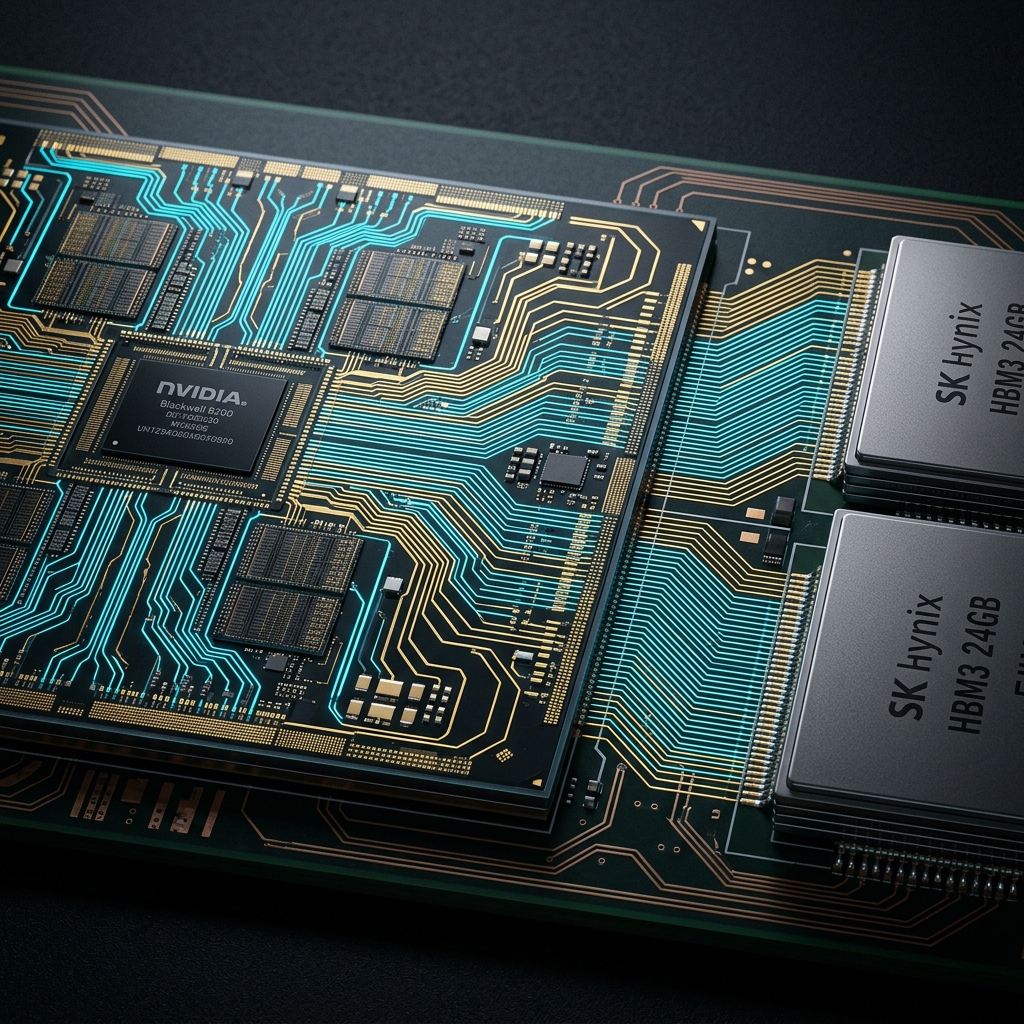
Technical Choke Points: Why These Tools Matter
The technological implications of this ban are profound. While much of the public discourse focuses on lithography—specifically ASML’s EUV and DUV systems—the manufacturing of a 7nm node is equally dependent on the specialized processes managed by the American ‘Big Three.’ Lam Research provides the atomic-layer etching (ALE) capabilities required to carve features at the near-atomic scale with extreme precision. Applied Materials dominates the chemical vapor deposition (CVD) and physical vapor deposition (PVD) markets; without their tools, constructing the intricate metal interconnects of a 7nm chip becomes an insurmountable engineering challenge.
KLA’s contribution is perhaps the most critical for mass production—their metrology and inspection systems allow engineers to identify defects that are invisible to anything else. Without the ability to monitor wafer-level variance in real-time, Hua Hong’s 7nm yields would likely remain at levels that are economically unviable. This blockade does not just delay Hua Hong; it effectively removes the technical foundation required to move beyond legacy nodes.
Geopolitical Fallout and the 2026 Competitive Landscape
This regulatory action comes at a pivotal moment in 2026, as the global semiconductor industry bifurcates into two distinct spheres. For Hua Hong, which has long been China’s second-largest foundry and a leader in mature-node power semiconductors, the transition to 7nm was a strategic imperative to remain relevant in the AI era. By cutting off these essential tools, the U.S.
is enforcing a technological ceiling on Chinese domestic manufacturing. For the American equipment giants, the loss of revenue from one of their largest clients is a significant financial headwind, yet the U.S. government has signaled that national security and technological containment outweigh the short-term quarterly earnings of the private sector.
As Hua Hong is forced to reconsider its entire 7nm roadmap, the gap between Chinese domestic capabilities and the leading-edge nodes produced by TSMC and Samsung is set to widen. The message from Washington is unequivocal: the tools of the future will not be shared with those who challenge the existing technological order. This maneuver secures a multi-year lead for Western and allied semiconductor interests, forcing China into a costly and uncertain path of developing domestic alternatives that are currently years behind the state-of-the-art.