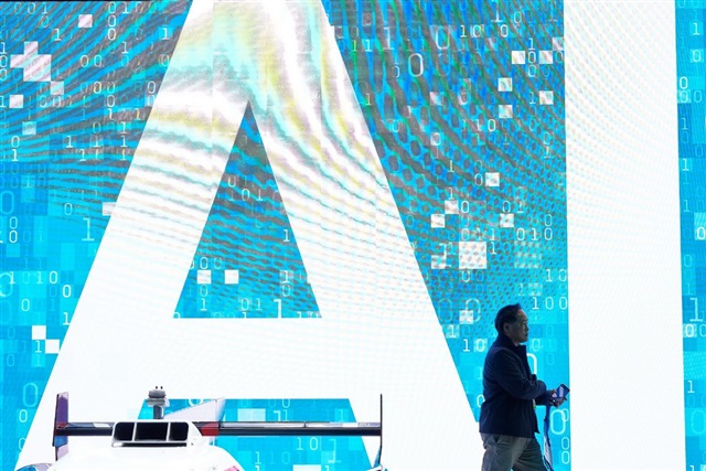
🔍 Executive Summary
- Episil Precision is aggressively reallocating its capital and production capacity toward large-diameter silicon epitaxy and silicon photonics, supported by a tripling of its Capex to meet 2027-2028 AI infrastructure roadmaps.
Strategic Deep-Dive
Episil Precision’s announcement to triple its capital expenditure (Capex) marks a seismic shift in the company’s operational strategy, reflecting the broader structural changes occurring within the AI hardware ecosystem. As the industry moves toward 2027 and 2028, the requirement for sophisticated interconnect solutions has never been higher. Episil’s strategic pivot toward large-diameter silicon epitaxy and silicon photonics is designed specifically to address the increasing complexities of AI data centers.
Silicon photonics, which integrates optical communication capabilities directly onto silicon substrates, is rapidly becoming the gold standard for high-speed data transmission, offering a pathway to bypass the physical limitations of traditional copper wiring. By tripling its investment, Episil is not just expanding capacity; it is fundamentally retooling its manufacturing floor to support the next generation of high-bandwidth AI accelerators. The company has made the difficult but necessary decision to phase out legacy, small-wafer lines that suffer from low margins and diminishing demand in the face of advanced manufacturing nodes.
Large-diameter wafers—typically moving toward 12-inch formats—provide significant economies of scale, allowing for more die per wafer and better compatibility with the automated processes of modern mega-foundries. This shift is critical for maintaining competitiveness as AI chip designers like Nvidia and Broadcom push for ever-denser integration of compute and communication. The technical logic behind this expansion is rooted in the ‘Optical I/O’ revolution.
As AI clusters scale to tens of thousands of GPUs, the energy cost of moving data between nodes becomes a dominant factor in total cost of ownership (TCO). Silicon photonics addresses this by using light to transmit data, drastically reducing latency and power consumption. Episil’s focus on high-quality epitaxy is essential here, as the material purity and crystal structure of the silicon layers directly determine the efficiency of the integrated optical components.
Furthermore, the 2027-2028 capacity roadmap demonstrates long-term vision, as the lead times for specialized semiconductor equipment continue to be a challenge. By securing this capacity now, Episil positions itself as an indispensable mid-stream partner for hyperscalers and chip designers who are already planning their infrastructure for the late 2020s. This aggressive Capex increase also signals a departure from volume-based commodity production toward high-value specialized manufacturing.
For investors and industry analysts, Episil’s transformation serves as a bellwether for the Taiwanese semiconductor sector’s ability to evolve. The success of this pivot will depend on the smooth execution of the new production lines and the continued demand for optical integration in AI workloads. If successful, Episil will move from being a peripheral components supplier to a core architect of the hardware that powers artificial intelligence, effectively future-proofing its business against the cyclical nature of traditional electronics markets.