🔍 Executive Summary
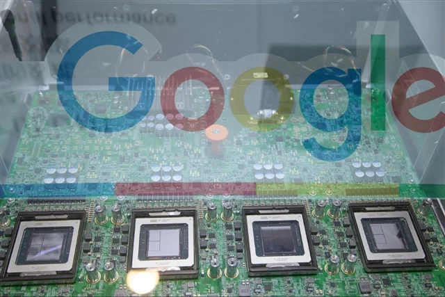
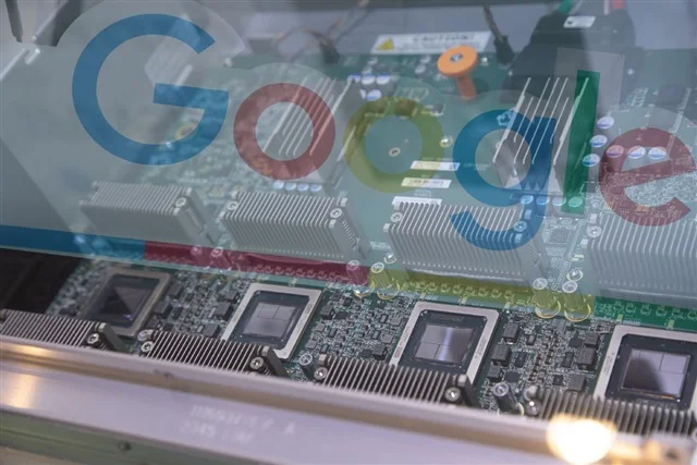
- Google has unveiled its 8th-generation Tensor Processing Units (TPUs), introducing a specialized split between the training-focused TPU 8t and the inference-optimized TPU 8i. This strategic pivot signals a definitive move away from universal accelerators toward Domain-Specific Architectures (DSA), aimed at eliminating bottlenecks throughout the AI model lifecycle and challenging Nvidia's general-purpose dominance.
Strategic Deep-Dive
Google’s announcement of its eighth-generation Tensor Processing Units (TPUs) marks a definitive and sophisticated shift in the evolution of AI hardware infrastructure. For the first time, Google is bifurcating its flagship AI accelerator into two distinct silicon variants: the TPU 8t, engineered for heavy-duty model training, and the TPU 8i, specifically tailored for high-efficiency inference. This divergence signals a departure from the ‘one-size-fits-all’ philosophy that has dominated the AI chip market for years, a paradigm largely led by Nvidia’s universal GPU architectures like the Hopper and Blackwell series.
By fully committing to Domain-Specific Architectures (DSA), Google is addressing the unique technical requirements of different stages in the AI model lifecycle. Training tasks require massive throughput, high precision, and seamless scaling across thousands of interconnected nodes. The TPU 8t addresses these with a restructured interconnect fabric and enhanced HBM management, allowing it to maintain high utilization rates even when training the world’s largest dense and MoE (Mixture of Experts) models.
In stark contrast, the TPU 8i is built to deliver deterministic low-latency responses. It prioritizes power efficiency and ‘quantization’ performance—using lower-precision data types like Int8 or Int4 to process requests rapidly without the massive energy consumption associated with training-grade silicon.
The 8th-generation TPU represents a full-stack optimization beyond the raw silicon. Google has redesigned the internal scheduling algorithms and memory layouts to ensure that each chip variant operates at its peak efficiency within Google’s specific software environment, such as JAX and TensorFlow. This holistic approach allows Google to bypass the structural bottlenecks inherent in general-purpose hardware.
As AI models become more complex and their deployment more ubiquitous, the efficiency gains provided by specialized silicon like the TPU 8t and 8i become a critical competitive advantage.
Furthermore, this strategy significantly reduces Google’s reliance on external vendors, providing tighter control over their operational costs and the carbon footprint of their massive data center fleet. While a universal GPU must maintain the hardware overhead necessary for any possible workload, Google’s specialized chips can shed redundant features, leading to higher performance per square millimeter of silicon. In the broader industry context, Google’s split strategy sets a new standard for hyper-scale cloud providers, potentially forcing a market-wide shift toward specialized AI acceleration as the only way to sustain the economic demands of the generative AI era.