🔍 Executive Summary
- ASML’s record €38.8 billion backlog secures its role as the industry gatekeeper, with the transition from High-NA to Hyper-NA lithography setting the stage for sub-2nm mass production.
Strategic Deep-Dive
ASML’s dominant position in the semiconductor lithography market remains unrivaled, as evidenced by its robust 2025 shipment data: 48 EUV systems and 131 immersion DUV tools. Generating €32.7 billion in annual revenue is an impressive feat, but the most telling metric for the industry’s future is ASML’s staggering €38.8 billion order backlog. This backlog serves as a vital barometer for global fab expansion, specifically underpinning critical projects such as Intel’s 18A push and TSMC’s massive capacity build-out in Arizona.
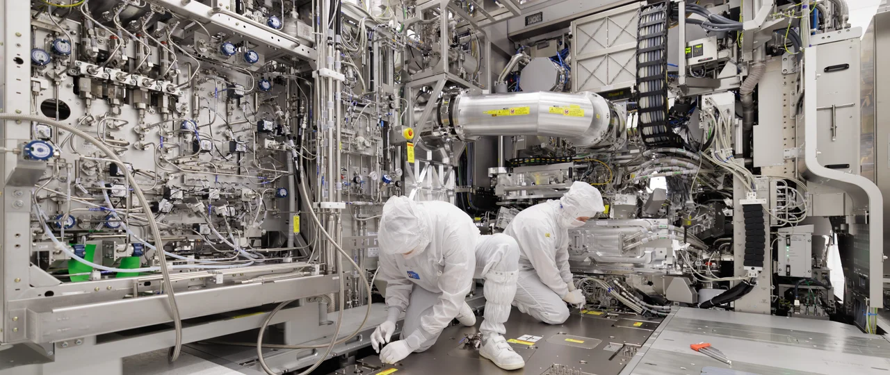
ASML is effectively the bottleneck through which all advanced node progress must pass. The company’s roadmap is defined by the leap from Low-NA (0.33 numerical aperture) to High-NA (0.55 NA), a transition that is essential for maintaining the scaling trajectory of Moore’s Law toward the 1.4nm node and beyond. High-NA EUV systems allow for significantly higher resolution, enabling chips to be printed with fewer exposures and higher yields at sub-2nm geometries.
Beyond High-NA, ASML is already laying the groundwork for Hyper-NA, which will push the boundaries of physics even further. The sheer capital intensity and specialized knowledge required for these systems ensure that ASML remains the sole gatekeeper of the advanced node era. As AI processors demand ever-increasing transistor densities, the reliance on ASML’s lithography roadmap will only intensify, making the company’s backlog the ultimate leading indicator for the global semiconductor cycle in 2027 and 2028.