🔍 Executive Summary
- Intel's 18A-P process node introduces a critical 9% performance boost and a massive 50% improvement in thermal conductivity, aiming to solve heat issues in high-density AI and compute chips.
Strategic Deep-Dive
In a pivotal technical disclosure that aims to reshape the competitive landscape of semiconductor manufacturing, Intel has detailed the performance metrics of its advanced 18A-P process node. As the company pushes toward its goal of reclaiming the top spot in the global foundry market, the 18A-P node stands as the definitive expression of its engineering progress. This node is an optimized version of the 18A architecture, specifically refined to meet the rigorous demands of next-generation high-performance computing (HPC) and mobile architectures.
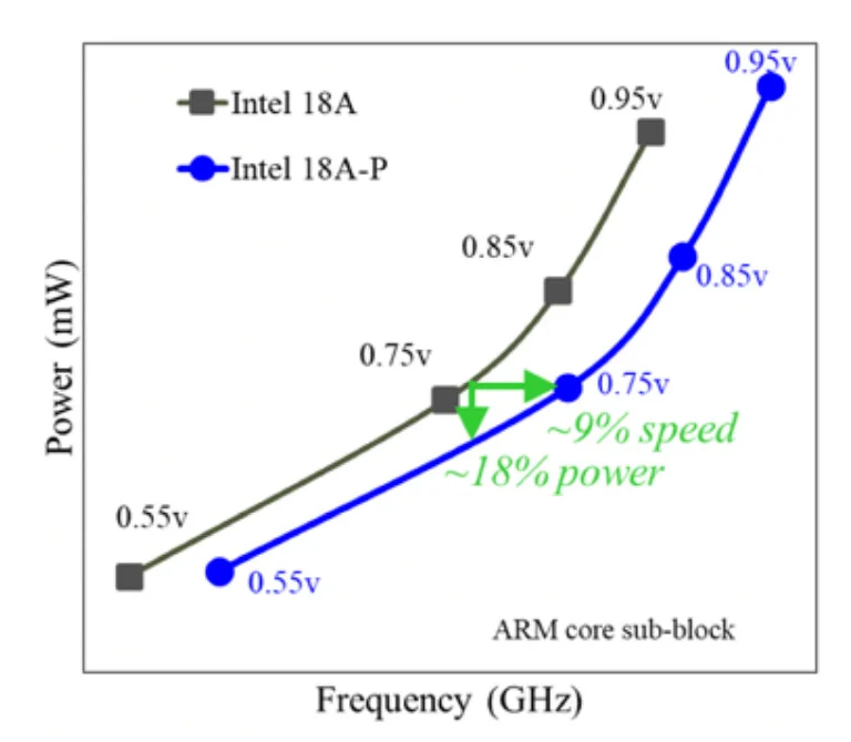
According to the technical brief, the 18A-P delivers a 9% increase in raw performance over the standard 18A node, while simultaneously achieving a reduction in total power consumption—a feat that highlights Intel’s mastery of the FinFET and Gate-All-Around (GAA) transition.
Beyond simple speed increases, the standout specification of the 18A-P node is a remarkable 50% improvement in thermal conductivity. As transistor dimensions shrink to the sub-2nm level, the density of heat generation becomes the primary bottleneck for sustained performance. By re-engineering the interconnect layers and material compositions within the die structure, Intel has managed to accelerate the movement of heat away from the logic gates at a rate 50% faster than previous benchmarks.
This thermal breakthrough is critical for the AI era; chips running intensive generative AI workloads can maintain peak clock speeds for longer durations without being forced into thermal throttling. For potential foundry clients building massive scale-out infrastructures, this translates to better total cost of ownership (TCO) through reduced cooling requirements and higher reliable uptime.
Intel’s disclosure also places a heavy emphasis on manufacturing maturity and economic viability. The company reports significant strides in reducing process variability—the subtle differences in transistor performance across a single wafer—and an overall improvement in yields. For a foundry service provider, yield is the lifeblood of the business; higher yields mean lower costs for customers and more predictable delivery timelines.
By focusing on these industrial-grade metrics, Intel is signaling to the market that 18A-P is not just a laboratory achievement but a production-ready platform capable of supporting the world’s most demanding hyperscale partners. The reduction in variability is particularly important for ensuring that every chip in a thousand-unit order performs identically, which is a key requirement for modern cloud computing environments.
As the industry watches the battle between Intel, TSMC, and Samsung, the 18A-P node represents Intel’s strongest case for technical parity. The focus on thermals and yield indicates that Intel has listened to the concerns of third-party chip designers who require more than just raw speed. By providing a node that runs cooler and produces more functional dies per wafer, Intel is positioning itself as a high-reliability alternative in the leading-edge semiconductor space.
This technical roadmap, if executed without delay, provides a clear path for Intel to attract the high-volume contracts necessary to sustain its massive multi-billion dollar fab investments and secure its future as a cornerstone of the global hardware supply chain.