🔍 Executive Summary
- JEDEC has achieved critical milestones for high-performance computing by publishing the DDR5 MDB standard and advancing the MRCD specification to facilitate the transition to Multiplexed Rank DIMM (MRDIMM) architectures.
Strategic Deep-Dive
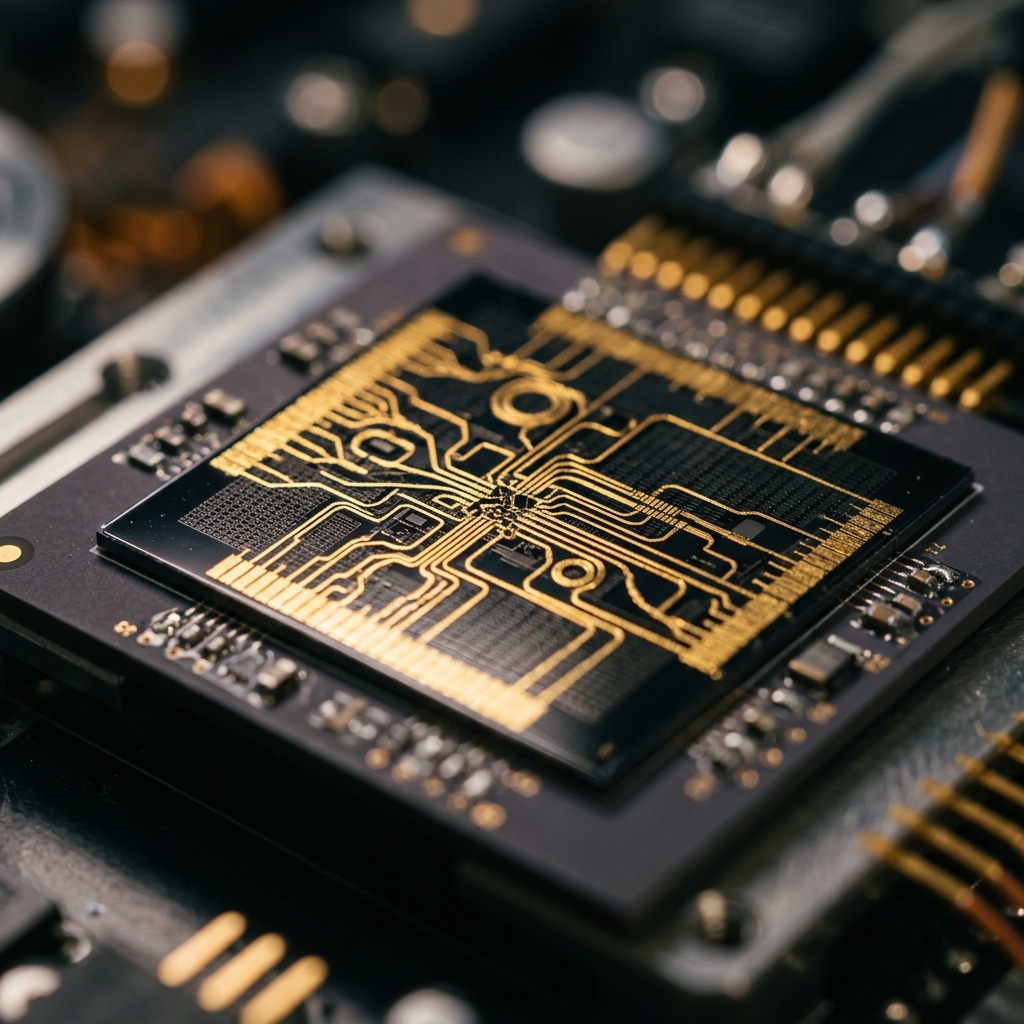
The JEDEC Solid State Technology Association has announced a series of pivotal milestones that define the trajectory of high-performance memory systems, addressing the critical bandwidth demands of the modern artificial intelligence era. Through the collaborative efforts of the JC-40 Committee for Logic and the JC-45 Committee for DRAM Modules, JEDEC has officially published the new DDR5 multiplexed rank data buffer (MDB) standard. This development is complemented by significant progress toward the finalization of the multiplexed rank registering clock driver (MRCD) standard, both of which are central components of the evolving DDR5 Multiplexed Rank Dual Inline Memory Module (MRDIMM) ecosystem.
The introduction of the MDB standard represents a sophisticated leap in interface logic. As data centers and AI training clusters demand increasingly higher memory bandwidth, traditional DDR5 scaling faces physical barriers in terms of signal integrity and pin density. The MDB facilitates a more efficient handling of data across multiple ranks by effectively doubling the data rate visible to the system controller without requiring a proportional increase in physical pins.
This is achieved through advanced multiplexing logic that aggregates signals from two independent ranks into a single high-speed channel. This logic-level innovation ensures that high-speed data paths remain stable and reliable under the intense thermal and electrical stresses found in modern AI server environments where temperatures and voltages fluctuate rapidly.
Furthermore, the advancements in the MRCD standard underscore JEDEC’s commitment to a holistic architecture for MRDIMMs. By refining how clock signals are registered and distributed across multiplexed ranks, the MRCD ensures precise timing synchronization. This synchronization is critical for maintaining low latency while operating at the elevated frequencies that MRDIMMs target, which can exceed 8800MT/s.
The physical layer of the MRCD is designed to mitigate the effects of jitter and skew that naturally occur when driving multiple DRAM loads. The synergy between MDB and MRCD is what enables the roadmap expansion JEDEC is currently pursuing, providing a standardized framework that memory manufacturers like Samsung, SK Hynix, and Micron, as well as system integrators, can rely upon for cross-platform interoperability.
From a data analytics perspective, the importance of this standardization cannot be overstated. By formalizing the interface logic, JEDEC is effectively reducing the R&D overhead for the entire microelectronics sector. The transition to MRDIMM technology is no longer a conceptual goal but a structured reality supported by formalized specifications.
This standardization is particularly vital for the growth of high-performance computing (HPC) and generative AI, where memory bandwidth—rather than raw compute power—has become the primary bottleneck. As we look toward the 2026-2027 window, these standards will dictate the cost-performance ratio of enterprise servers. By establishing these benchmarks early, JEDEC ensures that the industry avoids the fragmentation of proprietary solutions, fostering an environment where innovation in logic and DRAM can evolve in lockstep.
The continued work on the DDR5 roadmap by the JC-40 and JC-45 committees remains the cornerstone of server-grade memory evolution, ensuring that the global tech infrastructure is prepared for the next generation of computational challenges.