🔍 Executive Summary
- Samsung's foundry business is regaining its competitive edge as 4nm yields surpass the 80% milestone. This stability, combined with increasing demand for HBM4 base-dies, is driving a significant recovery in fab utilization and customer trust.
Strategic Deep-Dive
Samsung Electronics is signaling a robust recovery in its foundry division, with industry intelligence indicating that its 4nm process yield has officially surpassed the critical 80% threshold. This development marks a significant departure from previous years, where the company struggled with manufacturing consistency on its advanced nodes, leading to market share losses. Reaching an 80% yield is more than just a technical achievement; it represents the maturation of the manufacturing ecosystem, allowing for predictable pricing and reliable delivery schedules—factors that are paramount for global fabless customers in the high-stakes mobile and AI sectors.
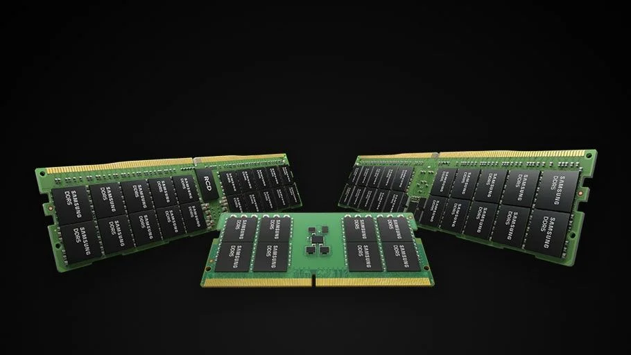
The strategic timing of this yield stabilization coincides with a pivotal shift in memory architecture: the arrival of HBM4. Unlike its predecessors, HBM4 necessitates a fundamental change in the ‘base-die’ located at the bottom of the memory stack. To meet the performance requirements of next-generation AI accelerators, these base-dies are shifting from traditional memory-based manufacturing to advanced logic foundry processes.
Samsung, as the world’s preeminent Integrated Device Manufacturer (IDM), is uniquely positioned to capitalize on this trend. By utilizing its stabilized 4nm logic process for the base-die and integrating it with its own HBM stack, Samsung can offer a turnkey solution that reduces supply chain complexity and optimizes performance for clients like NVIDIA, AMD, and various hyperscalers.
Analysts project that this synergy will be the primary vehicle for Samsung to claw back market share from TSMC. While TSMC remains the leader in pure-play foundry services, Samsung’s ability to synchronize logic and memory development under one roof provides a compelling value proposition in an era where data-transfer speeds between memory and processors are the primary bottleneck. Furthermore, the 4nm success serves as a critical technical validation for Samsung’s future roadmap, particularly its transition to 3nm Gate-All-Around (GAA) technology.
If Samsung can maintain this momentum and prove that it has solved its historical yield issues, it may trigger a shift in the global foundry landscape as customers seek to diversify their supply chains away from a single-source dependency on Taiwan. The reported increase in fab utilization rates suggests that global technology firms are already beginning to act on this newfound reliability, positioning Samsung as a vital pillar in the global AI hardware infrastructure.