🔍 Executive Summary
- ADTechnology has secured a significant KRW 40 billion contract to provide a full turnkey solution for US-bound AI data center SoC chiplets, utilizing Samsung Foundry's mature 4nm node.
Strategic Deep-Dive
The Turnkey Evolution: ADTechnology’s Strategic Breakthrough
ADTechnology’s announcement of a KRW 40 billion (approximately US$27.1 million) contract marks a significant milestone for South Korea’s fabless-support ecosystem. The agreement with an undisclosed US-based AI fabless firm targets the development and supply of high-performance computing (HPC) System-on-Chip (SoC) chiplets tailored for AI data center infrastructure. What elevates this deal above typical design services is its ’turnkey’ nature.
ADTechnology is now moving beyond its legacy role as a design assistant to become a comprehensive production partner—managing everything from high-level architecture and GDS-II physical design to final silicon supply. This transition demonstrates the growing maturity of Design Solution Partners (DSP) within the Samsung Foundry ecosystem and their ability to handle massive, complex projects for top-tier international clients.
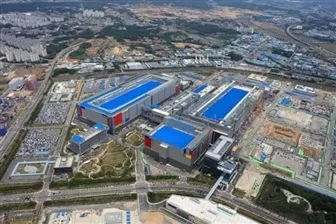
Technical Core: Samsung Foundry’s 4nm Node and Chiplet Integration
At the heart of this deal is Samsung Foundry’s advanced 4nm (SF4) process technology. As the semiconductor industry hits the limits of monolithic die scaling, the industry is pivoting toward ‘chiplet’ architectures. By breaking down a massive processor into smaller, specialized functional dies, designers can optimize each component for better yields and performance.
For the US client’s AI data center needs, this approach is essential. Large-scale AI inference requires massive parallel throughput and high-speed data movement, both of which are facilitated by Samsung’s 4nm node and its advanced packaging interconnects, such as the I-Cube technology. ADTechnology’s role involves ensuring that these disparate chiplets communicate with ultra-low latency and minimal power overhead—a challenge that requires deep architectural expertise in logic design and signal integrity.
Geopolitical Context and the ‘China-Plus-One’ Strategy
The global semiconductor landscape is undergoing a radical shift as companies seek to diversify their supply chains away from single-source dependencies. Amidst the ongoing US-China silicon tensions and the capacity constraints at TSMC, Samsung Foundry has emerged as the premier alternative for leading-edge logic fabrication. This contract proves that US fabless firms are increasingly confident in Samsung’s 4nm yields and ADTechnology’s ability to bridge the gap between abstract software requirements and physical silicon implementation.
For Samsung, this 4nm victory serves as a critical stepping stone toward securing trust for its future 3nm and 2nm Gate-All-Around (GAA) nodes. It reinforces the narrative that the Samsung Foundry ecosystem is ready to support the next wave of US-driven AI innovation with localized, reliable design support from partners like ADTechnology.
Future Implications for the HPC Market
As AI data centers demand more specialized, workload-optimized silicon, the era of general-purpose server CPUs is giving way to customized SoC solutions. The success of the ADTechnology-Samsung partnership in securing a KRW 40 billion US deal suggests that the barrier to entry for custom AI silicon is lowering for mid-sized fabless innovators. By leveraging the turnkey expertise of a DSP, these firms can bring highly advanced 4nm products to market without the massive internal overhead of a full-scale manufacturing team.
This democratization of high-end silicon design is likely to spur further innovation in the AI acceleration space, positioning South Korean design houses as the primary facilitators of the global AI infrastructure boom. The long-term impact will be a more resilient, multi-polar semiconductor supply chain where Samsung’s foundry technologies play a central role in powering the world’s most advanced data centers.