🔍 Executive Summary
- SK Hynix is recalibrating its investment strategy for the Cheongju M15X plant, potentially accelerating beyond 1b DRAM to adopt 6th-generation 1c nodes to meet the rapidly evolving requirements of the HBM4 supply chain.
Strategic Deep-Dive
The Strategic Pivot: From 1b to 1c at Cheongju M15X
SK Hynix is currently navigating a significant strategic crossroads regarding its M15X facility in Cheongju, South Korea. Initially envisioned as a high-volume manufacturing hub for fifth-generation 10nm-class (1b) DRAM, the plant’s roadmap is undergoing a critical re-evaluation. According to reports from ZDNet Korea and NewsPim, the company is weighing a shift toward sixth-generation 10nm-class (1c) DRAM.
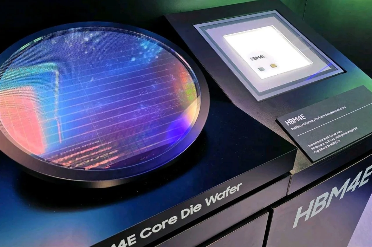
This potential transition is not merely a technical upgrade but a calculated response to the intensifying demands of the High-Bandwidth Memory (HBM) sector. As AI computing moves toward more complex architectures like HBM4, the underlying DRAM dies must satisfy increasingly stringent criteria for power efficiency and signal integrity, making the 1c node a non-negotiable asset for future leadership.
Technical Challenges: EUV Lithography and the 1c Node
The transition to the 1c node represents a formidable technical leap, primarily due to the increased reliance on Extreme Ultraviolet (EUV) lithography. While the 1b node integrated EUV to a certain extent, the 1c node requires a much more sophisticated application of these tools to achieve the required scaling. By utilizing EUV for more layers, SK Hynix aims to minimize patterning errors and improve the overall density of the memory cells.
This is particularly vital for the production of HBM base dies, which serve as the foundation for the 16-high stacked modules expected in the 2026-2027 timeframe. Skipping a prolonged 1b cycle at M15X allows SK Hynix to bypass potential oversupply in legacy nodes while securing the ‘first-mover’ advantage in the next premium tier of the memory market.
Competitive Landscape and HBM4 Readiness
This shift is also a preemptive strike in the escalating rivalry with Samsung Electronics and Micron. Both competitors have announced aggressive roadmaps for their 1c DRAM nodes, creating a high-stakes environment where being first to mass production can dictate market share for the next three to five years. For SK Hynix, M15X is the centerpiece of this battle.
By dedicating this advanced facility to 1c production, the company is ensuring it has the capacity to support the massive volume requirements of major AI chipmakers. The decision highlights a broader trend in the semiconductor industry: the ‘gold rush’ for AI silicon has compressed the traditional decade-long product cycles into a matter of years, forcing manufacturers to take bold risks with their capital expenditure to remain relevant.
Financial Implications and Long-term Viability
From a data architect’s perspective, the move to 1c DRAM is essential for overcoming the ‘memory wall’ in AI systems. The higher bit density and reduced power leakage of the 1c process translate directly into lower operational costs for data centers. While the initial investment in M15X to support 1c—including the installation of additional EUV scanners and the recalibration of cleanroom environments—will be substantially higher than the 1b alternative, the long-term ROI is projected to be superior.
If successful, this strategic acceleration will allow SK Hynix to dominate the HBM4 era with a more efficient, higher-performing product line, effectively turning the M15X facility into the most advanced memory fab on the planet and securing the company’s fiscal stability through the end of the decade.