🔍 Executive Summary
- Japanese material giant JSR is set to build its first photoresist plant in Taiwan to co-develop advanced resists with TSMC. Aiming for a 2028 operational date, the facility seeks to eliminate supply chain latency for next-generation lithography processes.
Strategic Deep-Dive
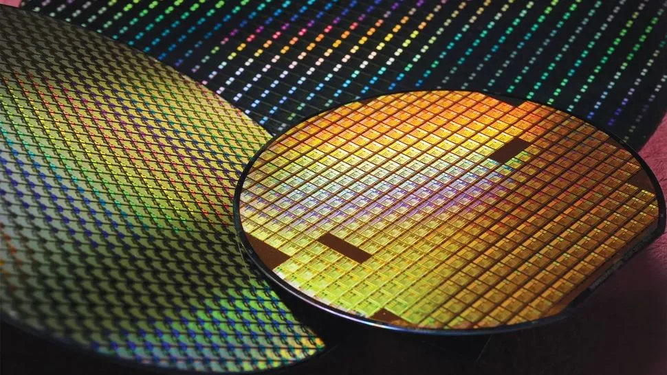
JSR’s decision to establish its first dedicated photoresist plant in Taiwan marks a critical intervention in the ‘Material Science Bottleneck’ that currently threatens the scaling of sub-2nm nodes. The multi-million dollar facility, scheduled for completion in 2028, is specifically designed to facilitate the co-development of next-generation photoresists in tandem with TSMC’s aggressive lithography roadmaps. As we push toward 2nm and 1.4nm processes, the physics of lithography becomes increasingly volatile.
Specifically, the industry faces the challenge of ‘stochastic effects’—random variations in photon absorption that can cause catastrophic defects at the molecular level. Solving these issues requires a tight, real-time feedback loop between the chemical synthesis at JSR and the wafer exposure at TSMC’s fabs. Historically, JSR operated at a competitive disadvantage in Taiwan compared to Japanese rivals like Shin-Etsu or SUMCO, who maintained more robust local infrastructures.
By localizing production, JSR eliminates the latency of trans-Pacific supply chains and allows for the custom-tailoring of resist chemistry to the specific quirks of TSMC’s Extreme Ultraviolet (EUV) and High-NA EUV machinery. This move underscores the growing importance of the ‘Cluster Effect,’ where the complexity of sub-2nm manufacturing mandates that material suppliers be geographically tethered to the foundry. In this high-stakes environment, being ‘just-in-time’ is no longer enough; suppliers must be ‘just-in-place.’ JSR’s localized presence ensures that material formulations can be tweaked on a weekly or even daily basis to maximize yield as new nodes transition from R&D to mass production.
This strategic alignment secures JSR’s position within the critical path of the world’s most advanced semiconductor manufacturing and signals a broader trend: the global semiconductor map is being redrawn around hyper-localized clusters where materials, logic, and packaging are physically integrated into a single, seamless ecosystem.