🔍 Executive Summary
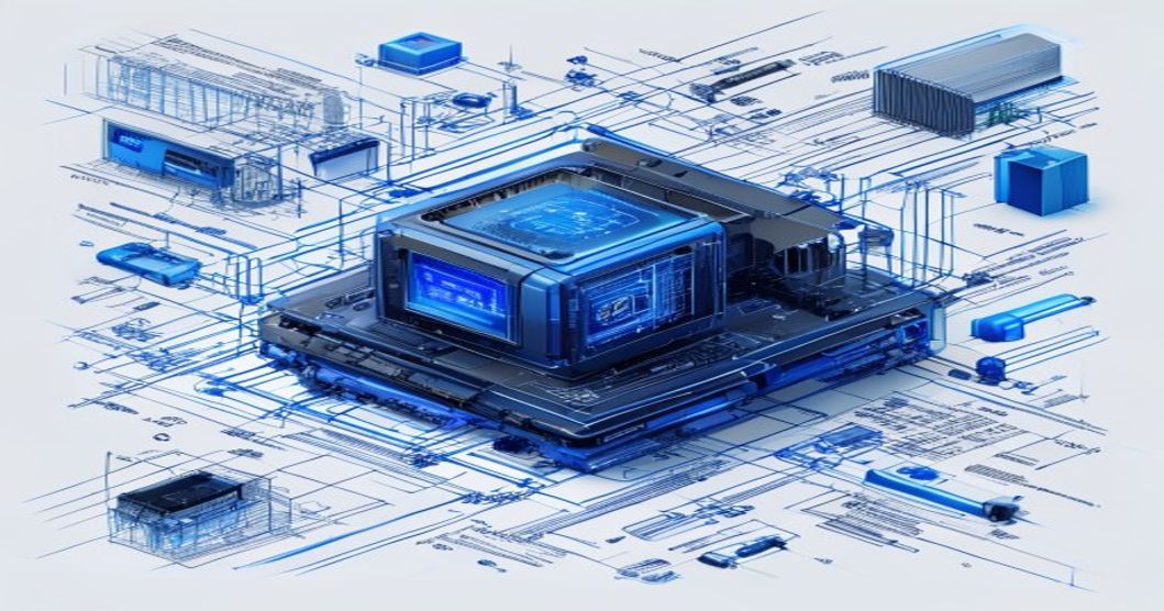
- Rambus has unveiled its cutting-edge PCIe 7.0 Switch IP, utilizing Time Division Multiplexing (TDM) to meet the 128 GT/s throughput requirements of next-generation AI and HPC fabrics.
Strategic Deep-Dive
As the demand for computational throughput reaches unprecedented heights, Rambus Inc. has addressed the industry’s most pressing hardware challenge with the launch of its PCIe 7.0 Switch IP. This sophisticated interconnect solution is designed to handle the massive data flows inherent in large language model (LLM) training and inference, providing a robust pathway for the next generation of data center architecture.
The cornerstone of this release is the integration of Time Division Multiplexing (TDM), a technology that effectively slices the time domain of communication lanes to allow for more efficient and lower-latency data transmission across a vast fabric of processors and accelerators.
In the transition from PCIe 6.0 to PCIe 7.0, the industry faces significant signal integrity hurdles. At 128 GT/s per lane, the physical limits of copper traces and board materials are being tested. Rambus’s implementation of TDM provides a critical solution to these challenges.
By multiplexing data streams based on time slots rather than just relying on raw frequency increases, the IP ensures high-density lane utilization without the catastrophic signal degradation often seen in high-frequency switching. This is particularly vital for the ‘scale-up’ and ‘scale-out’ architectures used in modern AI clusters, where thousands of GPUs must maintain coherent memory access and rapid synchronization.
From a historical perspective, PCIe generations have typically focused on doubling bandwidth. However, the move to 7.0 represents a shift toward intelligent fabric management. The Rambus Switch IP provides the foundational building blocks for system architects to design low-latency switches that can seamlessly connect CPUs, GPUs, and CXL-attached memory expansion modules.
As we move toward 2026 and 2027, the ability to maintain a consistent 128 GT/s throughput across a chassis will separate market-leading server designs from the competition.
Why this matters for the broader ecosystem is clear: as AI models scale to trillions of parameters, the intra-rack communication becomes as critical as the compute itself. The Rambus PCIe 7.0 Switch IP allows for a more granular control of data flow, reducing the ’tail latency’ that often plagues distributed AI workloads. For cloud service providers (CSPs) and enterprise hardware vendors, adopting this IP means they can build systems that are not only faster but also more power-efficient per gigabyte of data moved.
This efficiency is paramount as data centers grapple with the rising energy costs and cooling requirements described in other industry reports. By doubling the performance of PCIe 6.0 while maintaining strict power and area budgets, Rambus is ensuring that the hardware foundation for the late 2020s AI boom remains stable and scalable. This IP release is the technical blueprint that will allow the visionary software of the next decade to run on the high-performance hardware of tomorrow.


