🔍 Executive Summary
- SK Hynix has officially broken ground on its Indiana advanced packaging facility, strategically timed to supply HBM for Nvidia’s next-generation Rubin-Ultra GPUs by 2028.
Strategic Deep-Dive
Groundbreaking in Indiana: A Strategic US Milestone
SK Hynix has officially commenced construction on its advanced packaging facility in Indiana, marking a transformative step in the globalization of High Bandwidth Memory (HBM) production. This multi-billion dollar project is a cornerstone of SK Hynix’s strategy to localize manufacturing and testing in the United States, bringing the production of critical AI memory closer to the world’s most influential semiconductor design houses. The groundbreaking ceremony signifies more than just a new factory; it represents a fundamental shift in the AI supply chain, moving advanced back-end processes—traditionally concentrated in Asia—onto American soil.
This move is strategically designed to capitalize on the incentives provided by the CHIPS and Science Act while fostering a deeper integration with the US-based AI ecosystem.
Synchronizing with Nvidia’s Rubin-Ultra Roadmap
The most critical aspect of the Indiana plant’s timeline is its alignment with Nvidia’s long-term product roadmap. The facility is targeted for operational status in 2028, a year that is expected to be defined by the launch of Nvidia’s Rubin-Ultra GPU architecture. As AI models scale into the trillions of parameters, the demand for memory bandwidth has surpassed the capabilities of traditional DDR or even standard HBM configurations.
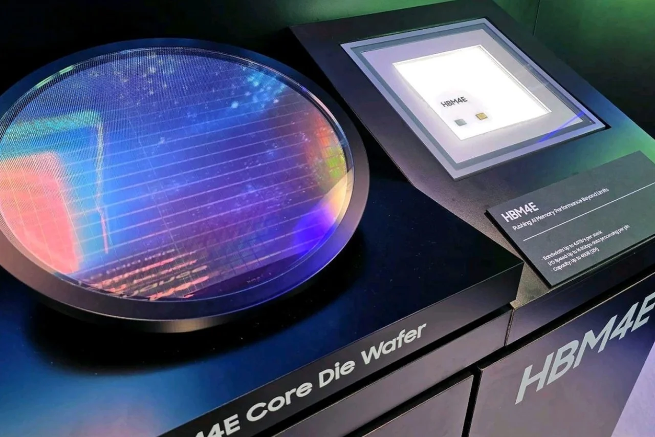
The Rubin-Ultra architecture will require the next generations of HBM (potentially HBM4 or beyond), characterized by unprecedented levels of vertical stack density and thermal efficiency. By timing the Indiana plant’s opening to coincide with this launch, SK Hynix ensures it will be the primary provider of ‘domestic’ HBM for Nvidia’s flagship AI processors, eliminating the logistical latency and customs complexities of trans-Pacific shipping during critical launch windows.
The Technical Importance of Advanced Packaging
Advanced packaging has become the new frontier of semiconductor innovation, particularly for HBM. Unlike standard memory, HBM relies on Through-Silicon Via (TSV) technology and sophisticated bonding processes like Mass Reflow Molded Underfill (MR-MUF) to stack DRAM dies vertically. These processes are incredibly delicate and define the final yield and performance of the memory module.
By performing these high-value tasks in Indiana, SK Hynix is bringing high-tech engineering jobs and specialized equipment to the region. This localized testing and packaging capability allow for faster feedback loops between SK Hynix and its customers, enabling rapid iteration of memory designs to suit the specific power and performance profiles of upcoming AI accelerators.
Geopolitical Resilience and Supply Chain Security
Establishing a manufacturing presence in the United States provides SK Hynix with a powerful buffer against geopolitical instability. In an era where trade tensions and regional conflicts can disrupt vital shipping lanes, having a fully functional production and testing hub in Indiana offers a level of supply chain resilience that is highly attractive to enterprise and government clients. This ‘on-shoring’ strategy ensures that the heart of the AI revolution remains secure and operational regardless of external market shocks.
For Nvidia and other US-based tech giants, the Indiana plant represents a reliable, secure source of the most critical component in their hardware stack. As the site progresses toward its 2028 operational goal, it solidifies SK Hynix’s position as an indispensable architect of the global AI infrastructure, bridging the gap between Korean memory expertise and American compute leadership.