🔍 Executive Summary
- On May 8, TSMC and Sony Semiconductor Solutions formalized an MOU to establish a joint venture in Kōshi, Kumamoto. This partnership aims to integrate TSMC's advanced logic fabrication with Sony's CMOS image sensor expertise, targeting high-growth sectors such as autonomous vehicles and robotics through on-chip AI processing capabilities.
Strategic Deep-Dive
A Paradigm Shift in Machine Vision: The Fusion of Logic and Optics
The strategic partnership between TSMC and Sony Semiconductor Solutions, formalized on May 8 through a non-binding MOU, marks a significant evolution in the semiconductor industry. The centerpiece of this joint venture (JV) is the development of next-generation AI image sensors that move beyond traditional light capture. By leveraging TSMC’s advanced logic process technology and Sony’s industry-leading Complementary Metal-Oxide-Semiconductor (CMOS) sensor architecture, the JV intends to pioneer a ‘stacked’ sensor design.
In this configuration, a specialized AI logic layer is bonded directly beneath the sensor pixels. This architectural integration allows for high-speed, on-chip data processing—enabling the sensor to identify objects and detect motion without sending raw data to a central processor. This transition to ‘Edge AI’ is critical for reducing latency and enhancing privacy in a data-driven world.
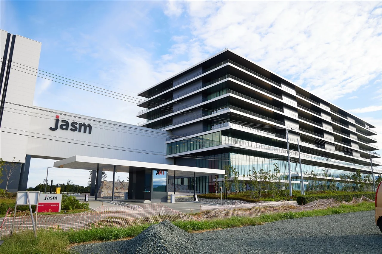
Kumamoto as the New Epicenter of Global Semiconductor Manufacturing
The decision to headquarter the JV in Kōshi, Kumamoto Prefecture, reinforces the region’s transformation into a world-class semiconductor hub, often referred to as Japan’s ‘Silicon Island.’ Sony will hold a majority stake in the venture, ensuring that the strategic direction remains aligned with Japan’s long-term economic security and technological leadership. For TSMC, this represents a deepening of its operational roots in Japan, providing a stable manufacturing environment outside of the Taiwan Strait. The synergy is clear: Sony provides the visionary sensor designs and market access, while TSMC provides the fabrication prowess needed to implement complex AI logic at scale.
This facility will likely attract a secondary ecosystem of supply chain partners, further solidifying Japan’s resurgence in the high-end semiconductor manufacturing sector.
Targets: Autonomous Systems, Robotics, and the Smartphone Future
The JV is laser-focused on three transformative markets: Automotive, Robotics, and Advanced Consumer Electronics. In the automotive sector, real-time visual processing is the primary bottleneck for Level 4 and Level 5 autonomous driving. AI sensors that can process environmental data locally at the millisecond level are essential for safety-critical collision avoidance.
In the realm of robotics, these sensors will allow for more intuitive human-machine interaction through advanced gesture and spatial recognition. Furthermore, the premium smartphone market is increasingly defined by computational photography. By integrating AI directly into the sensor, future mobile devices can execute complex imaging algorithms—such as real-time low-light enhancement and semantic segmentation—with significantly lower power consumption.
This TSMC-Sony alliance effectively sets a new industry standard, forcing competitors to rethink their approach to sensing and processing integration in the AI era.