🔍 Executive Summary
- The strategic alliance between Sony and TSMC leverages advanced fabrication nodes to integrate logic and sensing layers, solidifying their dominance in the next-generation image sensor market across mobile and automotive sectors.
Strategic Deep-Dive
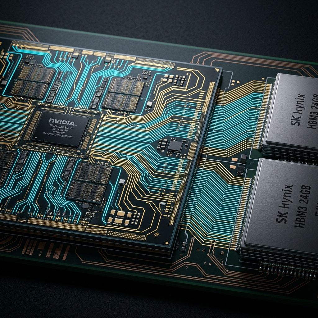
The partnership between Sony and TSMC represents a formidable convergence of design expertise and manufacturing excellence, creating a new benchmark in the global semiconductor industry. As the dominant leader in the CMOS image sensor (CIS) market, Sony is strategically aligning with TSMC to utilize the latter’s advanced fabrication nodes for the logic component of its next-generation sensors. This collaboration is specifically engineered to address the exploding demand for high-bandwidth, high-resolution imaging in the mobile, automotive, and industrial robotics sectors, where the ability to process visual data at the edge is becoming a critical differentiator.
Technically, the synergy focuses on the sophisticated integration of sensing and logic layers within a stacked sensor architecture. By outsourcing the logic wafer production to TSMC’s 22nm and 12/16nm specialized nodes, Sony can enhance the computational power embedded directly behind the pixel array. This allows for ‘Wafer-on-Wafer’ (WoW) bonding and the implementation of sophisticated on-chip AI processing.
Such integration reduces latency between light capture and data interpretation, which is vital for the sub-millisecond response times required by Level 4 and Level 5 autonomous driving systems. Furthermore, TSMC’s advanced logic nodes offer significant improvements in energy efficiency and signal-to-noise performance, allowing Sony to maintain its lead over competitors like Samsung and Intel who are struggling to match this level of specialized vertical integration.
From a geopolitical perspective, the Sony-TSMC alliance strengthens the ‘Japan-Taiwan tech axis,’ creating a resilient supply chain that is insulated from regional instabilities. The collaboration through the JASM (Japan Advanced Semiconductor Manufacturing) facility in Kumamoto is a testament to this strategic alignment, as it brings TSMC’s world-class process management to Japanese soil. This partnership also serves as an economic hedge, allowing Sony to lock in the world’s most advanced fabrication capacity while TSMC secures a steady, high-volume customer for its mature and specialized nodes.
As the world transitions toward a vision-centric digital economy—where every device from a smartphone to a factory robot requires ‘digital eyes’—Sony and TSMC are positioning themselves as the primary architects of this ecosystem. Their combined prowess ensures that they will remain at the top of the value chain, dictating the technical standards for the next generation of visual sensing hardware and securing a dominant market share against emerging players in the logic-sensing hybrid market.