🔍 Executive Summary
- TSMC is leveraging technical exclusivity and a transition to panel-level CoPoS packaging to maintain its lead in the AI semiconductor market, imposing strict controls on its Taiwan-based supply chain.
Strategic Deep-Dive
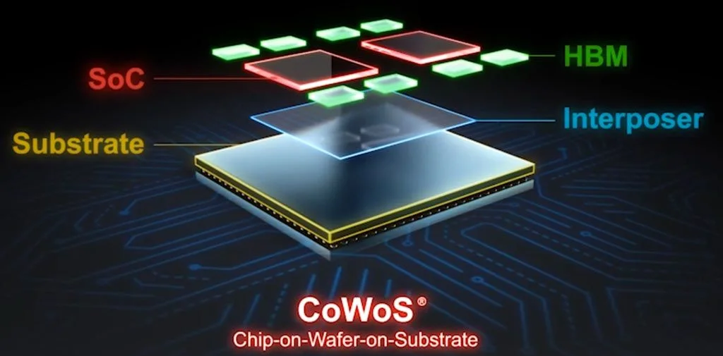
TSMC is strategically advancing its technological roadmap to maintain a commanding lead in the hyper-competitive AI semiconductor packaging market. The company is not merely scaling its established CoWoS (Chip on Wafer on Substrate) capacity to meet immediate hyperscale demand; it is aggressively pioneering the next frontier: CoPoS. This Panel-level Packaging (PLP) technology represents a significant architectural leap from traditional wafer-level methods.
By utilizing large rectangular panels instead of the standard 300mm circular silicon wafers, TSMC can achieve a much higher area utilization rate. This is particularly critical for the next generation of AI accelerators that integrate multiple HBM (High Bandwidth Memory) stacks with massive logic dies. The rectangular format minimizes edge waste and allows for a higher density of heterogeneous integration, which is essential for maintaining signal integrity and power efficiency in chips with massive I/O counts.
To safeguard this technological advantage, TSMC has instituted a rigorous regime of exclusivity and confidentiality within its domestic ecosystem. Reports indicate that the company has imposed strict non-disclosure agreements and exclusive supply mandates on its Taiwan-based equipment and materials partners. This move is a calculated attempt to create a ’technological moat,’ preventing rivals such as Samsung and Intel from gaining access to the specialized lithography tools, redistribution layer (RDL) materials, and substrate handling systems required for CoPoS.
By keeping the manufacturing know-how concentrated within a loyal network of domestic suppliers, TSMC effectively slows the progress of competitors who are attempting to develop their own PLP solutions to capture the AI market.
The transition to CoPoS also reflects a broader industry trend where the complexity of back-end packaging now rivals front-end wafer fabrication. As Moore’s Law approaches its physical and economic limits, advanced packaging provides the necessary performance gains through the integration of multiple chiplets into a single package. TSMC’s strategy of locking in the supply chain ensures that it remains the sole provider capable of delivering the interconnect density and thermal performance required for high-end AI processors.
This control over the advanced packaging segment is a defensive masterstroke, ensuring that even if competitors can match TSMC’s logic node performance, they will struggle to match its holistic system-in-package (SiP) capabilities, thereby maintaining TSMC’s position as the indispensable partner for the world’s leading AI chip designers.