🔍 Executive Summary
- Vanguard International Semiconductor (VIS) reports that AI infrastructure buildouts are driving capacity constraints and higher pricing, leading to an accelerated sampling schedule for its new 12-inch fab in Singapore to meet 2026 market demands.
Strategic Deep-Dive
Strategic Pivot: The 2026 Semiconductor Landscape and VIS’s Aggressive Expansion
As the semiconductor industry navigates the complexities of the mid-2020s, Vanguard International Semiconductor (VIS) has identified a clear decoupling between general macroeconomic sentiment and the specific, high-velocity growth of artificial intelligence. According to recent executive disclosures, the sheer volume of AI-driven demand has effectively neutralized the volatility associated with ongoing geopolitical tensions. In this high-stakes environment, the traditional 8-inch foundry model, while reliable, is being increasingly marginalized by the stringent performance and power efficiency requirements of AI infrastructure.
VIS is responding by fast-tracking its transition to 12-inch wafer production, signaling a fundamental shift in its operational DNA.
The Singapore Strategic Buffer and Sampling Timeline
The acceleration of the Singapore 12-inch fab schedule is a landmark indicator of current market urgency. By shifting the sampling phase to July 2026, VIS is positioning itself as a primary provider for next-generation power management ICs (PMICs) and high-performance analog chips. Singapore’s role as a technologically advanced, neutral hub provides a significant geopolitical buffer, allowing VIS to serve as a ‘Safe Haven’ for global chip designers who are increasingly wary of regional trade restrictions and supply chain fragility.
This strategic location enables VIS to capture high-margin orders from both Western and Eastern tech giants who require reliable, non-disruptive capacity for their AI training and inference hardware.
Capacity Crowding and the Economics of AI Nodes
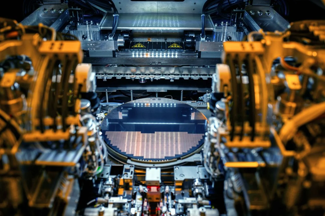
One of the most profound impacts of the AI infrastructure boom is the phenomenon of ‘capacity crowding.’ As major cloud service providers (CSPs) and GPU manufacturers secure long-term supply agreements, the available foundry space for traditional consumer electronics has tightened significantly. This has created a natural upward trajectory in average selling prices (ASPs), which VIS is strategically leveraging. The new 12-inch facility is specifically optimized for high-voltage and Bipolar-CMOS-DMOS (BCD) processes.
These are essential for the sophisticated power delivery systems required by AI clusters that consume tens of kilowatts per rack.
Moving to 12-inch wafers allows for more than just a volume increase; it facilitates the integration of more complex features on a single die, reducing the overall footprint and heat signature of the power components. As we progress through the second half of 2026, the success of VIS will depend on its ability to maintain this accelerated execution. The market is witnessing a fundamental re-rating of foundry assets where physical capacity in stable, high-tech regions like Singapore is becoming the ultimate currency.
VIS’s move from legacy node dominance to the high-performance demands of the AI era represents a high-conviction bet on the permanence of the accelerated computing transition.