🔍 Executive Summary
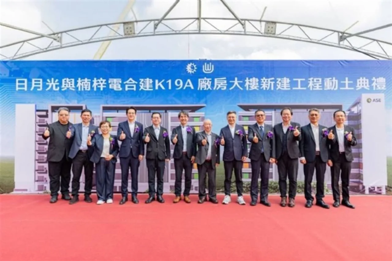
- Global OSAT leader ASE and PCB specialist Wus Printed Circuit have entered a joint venture to build a sophisticated backend facility in Kaohsiung.
- The project targets a September 2029 operational launch to mitigate the persistent supply-demand imbalance in the AI chip market.
- The facility is strategically positioned within the Nanzih Technology Industrial Park to leverage Taiwan’s Southern Semiconductor S-Corridor.
Strategic Deep-Dive
In a transformative move that underscores the critical importance of backend synergy in the artificial intelligence era, Advanced Semiconductor Engineering (ASE), the world’s preeminent semiconductor assembly and testing provider, has solidified a joint venture with Wus Printed Circuit. This strategic alliance is dedicated to the construction and operation of a massive advanced packaging facility in Kaohsiung, Taiwan, representing a significant escalation in the race to secure AI-ready production capacity. As AI-driven demand continues to outpace the industry’s current ability to deliver complex silicon modules, this partnership aims to bridge the gap by integrating ASE’s world-class packaging expertise with Wus’s high-end PCB and substrate capabilities.
The new facility, located in the strategically vital Kaohsiung Nanzih Technology Industrial Park, is slated for a grand opening and operational commencement in September 2029. This timeline is carefully calibrated to meet the projected maturity of next-generation AI architectures, which will rely heavily on chiplets and heterogeneous integration.
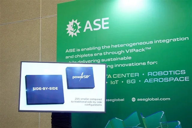
The technical scope of the project is immense. As the semiconductor landscape shifts toward High-Performance Computing (HPC), the reliance on advanced packaging technologies like CoWoS (Chip-on-Wafer-on-Substrate) and 3D IC has become absolute. By co-locating substrate intelligence with assembly processes, ASE and Wus intend to streamline the production of high-density interconnects required for modern GPU and TPU modules.
This vertical alignment not only optimizes the supply chain but also enhances overall yield rates for large-die packages that are notoriously difficult to manufacture. The investment is a cornerstone of Taiwan’s Southern Semiconductor S-Corridor initiative, which seeks to decentralize the semiconductor cluster from northern Taiwan and build a resilient, high-tech manufacturing belt in the south.
Furthermore, the long-term nature of this 2029 projection reflects a consensus among industry leaders that the AI boom is a multi-decade structural shift rather than a transient peak. Analysts suggest that by the time the Kaohsiung plant is fully operational, the demand for sophisticated backend solutions will have doubled, driven by the proliferation of edge AI and autonomous systems. For ASE, this joint venture is a defensive and offensive masterstroke; it secures a reliable supply of high-spec materials from Wus while simultaneously building a fortress of capacity that competitors will find difficult to match.
As geopolitical considerations continue to influence supply chain decisions, ASE’s decision to double down on its domestic footprint in Kaohsiung reinforces Taiwan’s status as the indispensable heart of the global semiconductor industry. The scale of this expansion is expected to attract a secondary layer of equipment suppliers and material science firms to the Nanzih region, effectively creating a self-sustaining ecosystem for advanced packaging that will serve global tech giants for years to come.