🔍 Executive Summary
- In response to the unprecedented demand for AI inference, Samsung Electronics is recalibrating its HBM roadmap to challenge SK Hynix's dominance, focusing on the technical integration of logic dies and HBM4 specifications by 2027.
Strategic Deep-Dive
The Architectural Pivot: From Generic Memory to Custom AI Storage
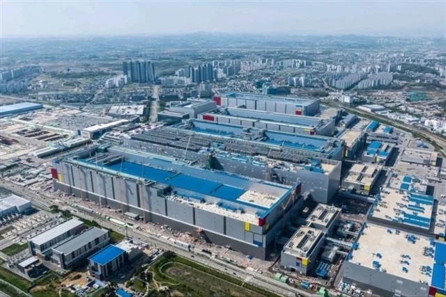
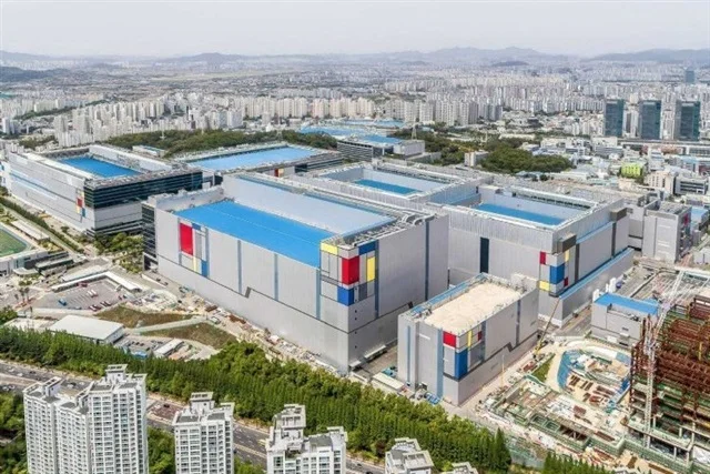
The global semiconductor landscape is witnessing a profound shift as the focus of AI deployments migrates from massive training clusters to high-throughput inference engines. This transition has placed an immense strain on existing memory architectures, necessitating a leap in bandwidth and a reduction in thermal resistance. Samsung Electronics, currently in a high-stakes chase to reclaim the market share held by SK Hynix, is strategically pivoting its resources toward the next-generation HBM4 standard.
The Data Architect’s perspective reveals that this is not merely an incremental update; it is a total overhaul of the interconnect topology between memory and the GPU/NPU. By targeting 2027 for full-scale mass production, Samsung is betting on a ‘custom HBM’ model where the base logic die is fabricated using advanced foundry nodes (4nm or below) to handle increasingly complex data management tasks right at the memory boundary.
Technical Contention: HBM3e Saturation and the Leap to HBM4
As current-generation HBM3e reaches its physical limits in terms of stack height and power delivery, the industry is looking toward HBM4 as the definitive solution for next-generation AI accelerators. Samsung’s strategy involves the implementation of advanced packaging techniques, specifically hybrid bonding and high-density Through-Silicon Vias (TSVs). Unlike traditional Microbumps, hybrid bonding allows for more direct copper-to-copper connections, significantly reducing the z-height of the package and improving thermal dissipation—a critical bottleneck in high-density AI server clusters.
This technical evolution is essential because as thermal throttling in high-density clusters becomes a more frequent occurrence, the ability to maintain peak performance under load becomes the primary metric of success for memory providers. Samsung’s 2027 roadmap explicitly addresses these architectural bottlenecks by integrating the logic die and memory stack into a more cohesive, high-efficiency unit.
Supply Chain Pressures and the Margin Expansion of DDR5
While the spotlight remains on HBM, the foundational market for DDR5 is undergoing its own transformation. Major manufacturers are operating at near-full capacity, creating a ripple effect across the entire hardware component supply chain. However, for a Data Architect, this capacity constraint is a double-edged sword.
On one hand, it limits the immediate availability of hardware for non-AI applications; on the other, it has led to significant margin improvements for advanced DDR5 products. Samsung is leveraging the yield stability of its 1c nm process to optimize these margins, using the resulting capital to fund the R&D required for the HBM4 transition. The competitive landscape between Samsung and SK Hynix is thus evolving into a multi-front war: a volume battle in the DDR5 space and a high-technology architectural battle in the HBM4 space.
The winner will be determined by who can most effectively balance current capacity pressures with the long-term goal of delivering specialized, low-latency AI storage solutions that can keep pace with the exponential growth of large language model parameters.