🔍 Executive Summary
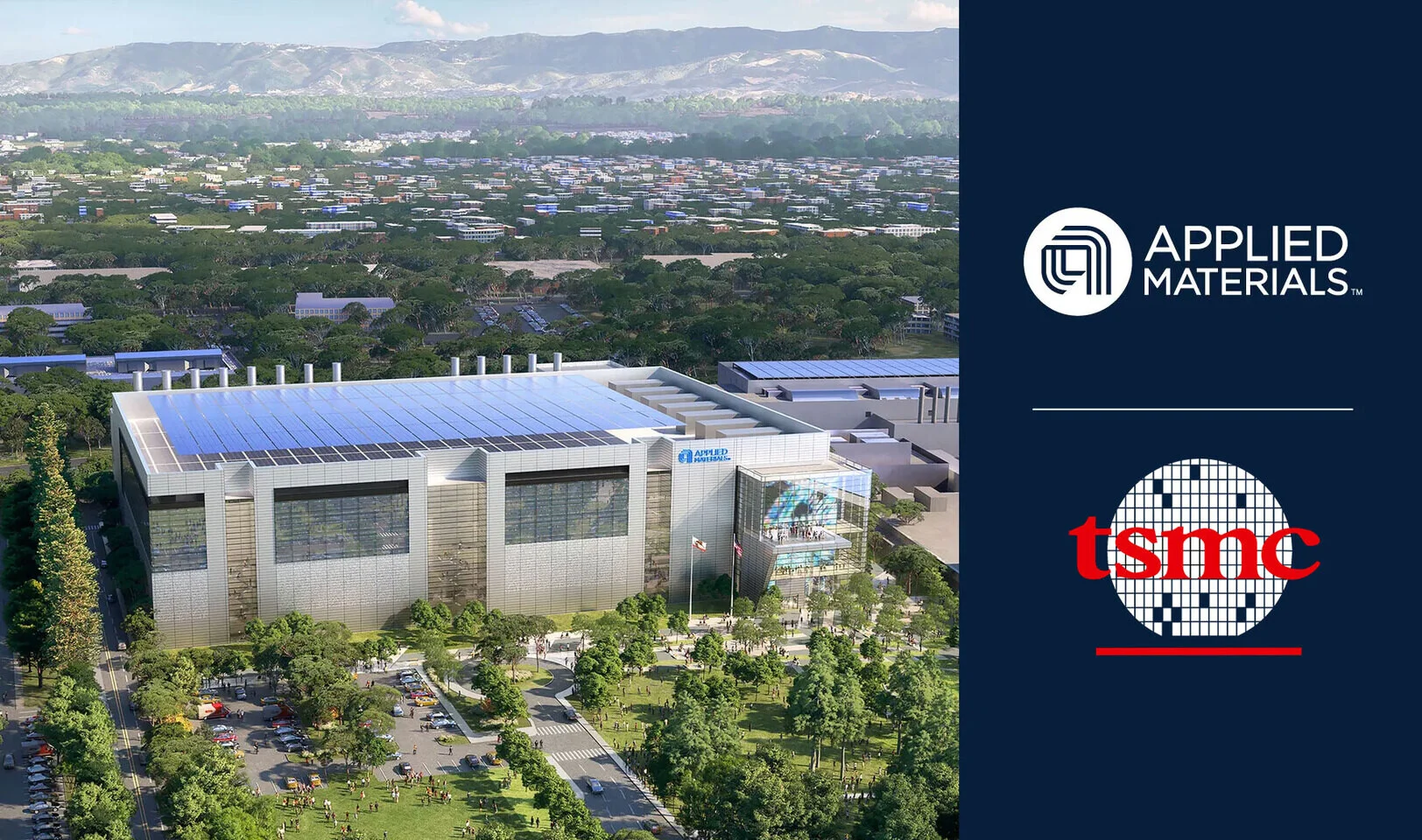
- Applied Materials and TSMC have solidified a landmark innovation partnership at the Equipment and Process Innovation and Commercialization (EPIC) Center in Silicon Valley. Building on three decades of collaboration, this alliance focuses on accelerating the transition from materials research to high-volume manufacturing for the AI era. By co-innovating on advanced materials engineering and equipment design, the two giants aim to overcome the physical bottlenecks of semiconductor scaling and secure the hardware foundation for future AI infrastructure.
Strategic Deep-Dive
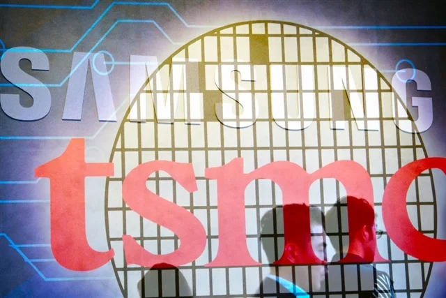
Applied Materials, Inc. and Taiwan Semiconductor Manufacturing Company (TSMC) have embarked on a transformative journey by establishing a strategic innovation alliance at the Equipment and Process Innovation and Commercialization (EPIC) Center. This collaboration, which commemorates over 30 years of shared history, is specifically designed to address the escalating complexities of semiconductor manufacturing in the artificial intelligence era.
Located in Silicon Valley, the EPIC Center serves as a high-velocity innovation hub where the two industry titans can co-develop materials, equipment, and process flows in a simulated production environment. As the industry approaches the limits of traditional planar and even FinFET scaling, the focus has shifted toward atomic-level materials engineering. The partnership is strategically aimed at the development of sub-2nm nodes, including the upcoming A14 and A10 architectures, where the integration of new conducting materials and low-k dielectrics becomes non-negotiable.
By leveraging Applied Materials’ expertise in atomic layer deposition (ALD) and chemical mechanical polishing (CMP) alongside TSMC’s mastery of high-volume foundry operations, the alliance intends to drastically reduce the cycle time between lab-scale breakthroughs and fab-ready commercialization. This is particularly vital for the production of massive AI accelerators and high-performance computing (HPC) processors that require unprecedented transistor density and power efficiency. Furthermore, the EPIC Center collaboration focuses on advanced packaging techniques—such as Chip-on-Wafer-on-Substrate (CoWoS)—which are essential for the next generation of AI hardware.
For TSMC, this early-access model to Applied’s latest toolsets ensures it can maintain its yield leadership at the bleeding edge. For Applied Materials, it provides a rigorous, real-world validation ground for its most ambitious engineering concepts. The synergy between these organizations is critical for overcoming the ‘red brick wall’ of the International Roadmap for Devices and Systems (IRDS).
As we transition into an era where materials engineering becomes the primary driver of performance gains, replacing traditional lithographic scaling, the Applied-TSMC alliance stands as a lighthouse for the entire semiconductor ecosystem, ensuring that the physical substrate of the AI revolution remains scalable, reliable, and commercially viable for years to come.