🔍 Executive Summary
- Japan is leading a global race to commercialize diamond semiconductors, with university-led startups initiating factory construction to produce high-power, radiation-hardened chips that could surpass the limits of current Silicon Carbide (SiC) technology by 2026.
Strategic Deep-Dive
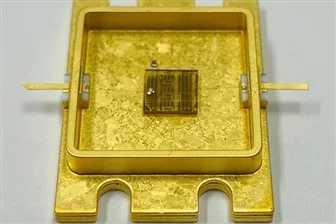
Japan is rapidly carving out a dominant position in the next frontier of power electronics: the commercialization of diamond semiconductors. While Silicon Carbide (SiC) and Gallium Nitride (GaN) are currently the darlings of the electric vehicle (EV) industry, diamond is widely regarded as the ‘ultimate semiconductor’ that will eventually succeed them. A robust ecosystem of Japanese university-backed startups is now moving beyond the laboratory, initiating factory construction and preparing for mass-scale sample production and device demonstrations targeted for 2026.
This transition signifies a shift from material science curiosity to industrial-grade hardware reality.
From a data systems and materials architecture perspective, the advantages of diamond are unparalleled. Its thermal conductivity is approximately 2,200 W/mK, which is more than five times that of SiC and twice that of pure copper. This allows diamond-based power modules to operate without the heavy, bulky liquid-cooling systems required by traditional silicon or even SiC devices.
Furthermore, diamond possesses an immense breakdown field (10 MV/cm) and a wide bandgap (5.5 eV), enabling it to handle voltages and temperatures that would incinerate conventional chips. For hardware architects, this means the ability to design much smaller, lighter, and more efficient power converters for extreme environments, such as deep-space satellites, geothermal energy extraction sensors, and nuclear reactor monitoring systems.
The technical hurdle has always been the synthesis of large-area, high-purity diamond wafers. Japanese startups are leading the way in optimizing Microwave Plasma Chemical Vapor Deposition (MPCVD) techniques to grow high-quality synthetic diamonds. By 2026, the roadmap includes the rollout of 2-inch and eventually 4-inch diamond wafers, which are critical for achieving the economies of scale necessary for commercial adoption.
These startups are also refining ion implantation and doping processes—historically difficult in diamond due to its extremely dense crystal lattice—to create functional transistors and diodes that can interface with modern electronic systems.
The strategic importance of Japan’s progress cannot be overstated. As the global semiconductor industry seeks materials that can push the limits of energy efficiency and radiation hardness, Japan is positioning itself as the primary source for diamond-based hardware. This development is particularly relevant for the aerospace and defense sectors, where ‘radiation hardening’ is a critical requirement.
A diamond-based communication satellite, for instance, could operate closer to the sun or in high-radiation orbits with significantly higher data throughput due to its superior thermal management and high-frequency capabilities. As we approach the 2026 production milestone, Japan’s diamond semiconductor industry is set to redefine the performance ceiling for high-end power management and specialized sensing applications.