🔍 Executive Summary
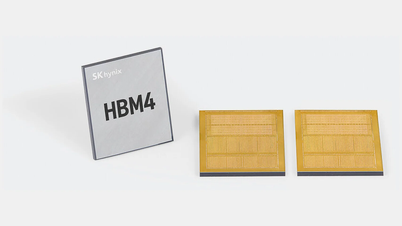
- In a strategic R&D alliance, SK hynix is adopting Intel's Embedded Multi-die Interconnect Bridge technology to redefine the HBM performance envelope.
Strategic Deep-Dive
The architecture of high-performance computing is undergoing a fundamental transformation, and at the center of this shift is the technical alliance between SK hynix and Intel. By integrating Intel’s proprietary Embedded Multi-die Interconnect Bridge (EMIB) 2.5D packaging technology into its High Bandwidth Memory (HBM) roadmap, SK hynix is signaling a departure from traditional industry silos toward a more integrated, foundry-agnostic supply chain. To understand the significance of this move, one must look at the physics of advanced packaging.
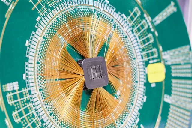
As AI models demand exponential increases in data throughput, the ‘memory wall’—the latency bottleneck between the processor and the memory—becomes the primary limiting factor. Traditional 2D packaging, where chips are placed side-by-side on a printed circuit board, is no longer sufficient. Intel’s EMIB technology offers a sophisticated alternative to the standard silicon interposer used in 2.5D packaging.
Instead of a large, expensive silicon slab covering the entire package, EMIB uses small, embedded silicon bridges that provide localized, high-density interconnects only where they are needed. This results in significantly lower signal latency, reduced power consumption, and improved thermal management—factors that are critical when stacking multiple layers of HBM near a high-wattage AI processor. SK hynix’s decision to explore EMIB for its HBM memory is a direct response to a changing market where customers are increasingly considering Intel Foundry for their next-generation chip designs.
By ensuring its HBM is fully optimized for Intel’s premier 2.5D packaging technology, SK hynix provides a seamless integration path for hyperscalers and semiconductor designers who are looking to diversify their manufacturing away from a single-source foundry model. Furthermore, this collaboration highlights the rising importance of ‘advanced packaging’ as a key differentiator in the post-Moore’s Law era. When the limits of silicon lithography are reached, the performance gains must come from how the components are interconnected.
SK hynix’s R&D efforts with Intel demonstrate a proactive stance in maintaining its market leadership by mastering multiple advanced packaging ecosystems. This technical synergy allows SK hynix to offer a more resilient and flexible supply chain, ensuring that its HBM remains the memory of choice regardless of which foundry ultimately manufactures the processor. In essence, the marriage of SK hynix’s world-class memory die with Intel’s cutting-edge interconnect technology represents the future of AI hardware—a future where the bridge is just as important as the chip it connects.